
EP2C35F672C6
| Part Description |
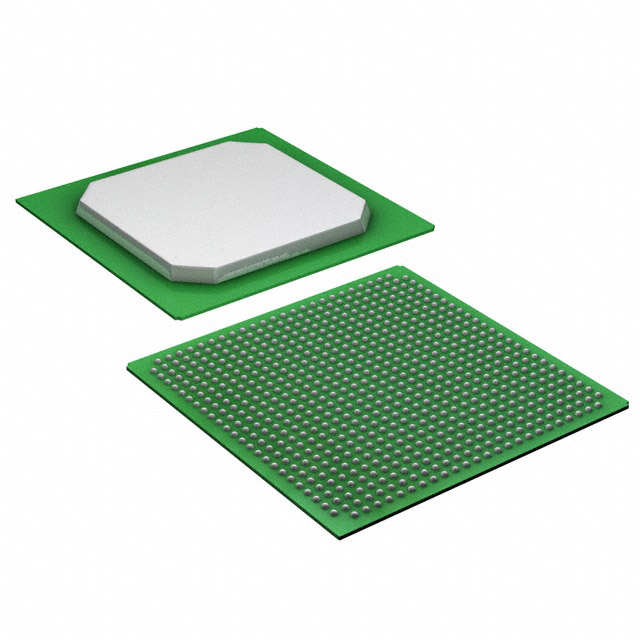
Cyclone® II Field Programmable Gate Array (FPGA) IC 475 483840 33216 672-BGA |
|---|---|
| Quantity | 874 Available (as of June 15, 2026) |

| Product Category | Field Programmable Gate Array (FPGA) |
|---|---|
| Manufacturer | Intel |
| Manufacturing Status | Active |
| Manufacturer Standard Lead Time | 8 Weeks |
| Datasheet |
Specifications & Environmental
| Device Package | 672-FBGA (27x27) | Grade | Commercial | Operating Temperature | 0°C – 85°C | ||
|---|---|---|---|---|---|---|---|
| Package / Case | 672-BGA | Number of I/O | 475 | Voltage | 1.15 V - 1.25 V | ||
| Mounting Method | Surface Mount | RoHS Compliance | RoHS non-compliant | REACH Compliance | REACH Unaffected | ||
| Moisture Sensitivity Level | 3 (168 Hours) | Number of LABs/CLBs | 2076 | Number of Logic Elements/Cells | 33216 | ||
| Number of Gates | N/A | ECCN | 3A991D | HTS Code | 8542.39.0001 | ||
| Qualification | N/A | Total RAM Bits | 483840 |
Overview of EP2C35F672C6 – Cyclone® II Field Programmable Gate Array (FPGA) IC 475 483840 33216 672-BGA
The EP2C35F672C6 is an Intel Cyclone® II FPGA provided in a 672-ball BGA package for surface-mount applications. It integrates 33,216 logic elements, approximately 0.48 Mbits of embedded memory, and 475 I/O pins to support mid-density programmable logic designs.
Designed for commercial-grade embedded and DSP-oriented applications, the device family datasheet documents architecture-level features such as global clock networks and PLLs, embedded multipliers, flexible I/O structure, and standard configuration and testing support.
Key Features
- Logic Capacity — 33,216 logic elements for implementing mid-density custom logic, state machines, and glue logic.
- Embedded Memory — 483,840 bits (approximately 0.48 Mbits) of on-chip RAM to support buffering, FIFOs, and embedded data storage.
- I/O Count — 475 general-purpose I/O pins to support wide parallel interfaces and multiple peripheral connections.
- Package — 672-ball BGA (672-FBGA, 27×27) surface-mount package for high pin count and compact board layout.
- Power — Core supply range from 1.15 V to 1.25 V to match Cyclone II core voltage requirements.
- Operating Range — Commercial operating temperature range of 0 °C to 85 °C.
- Configuration & Test — Family documentation includes IEEE 1149.1 (JTAG) boundary-scan support and configuration options for system-level integration.
- Clocking & DSP Support — Datasheet describes global clock networks, PLLs, and embedded multiplier blocks for DSP and timing-critical designs.
- Compliance — RoHS status: Compliant for lead-free manufacturing processes.
Typical Applications
- Embedded Processing — Low-cost embedded processing solutions where programmable logic and embedded memory are used to implement custom accelerators and control logic.
- Digital Signal Processing — Low-cost DSP solutions leveraging the family’s embedded multipliers and memory for signal filtering and arithmetic pipelines.
- High‑I/O Interface Bridging — Applications requiring dense I/O—parallel buses, multiple peripherals, or complex interface conversion—benefit from 475 I/O pins.
- External Memory Interfacing — Designs that require controlled external memory interfaces, supported by the family’s documented external memory interfacing features.
Unique Advantages
- High logic density in a compact package: 33,216 logic elements in a 672-BGA footprint help consolidate multiple functions into a single FPGA.
- Significant on-chip RAM: Approximately 0.48 Mbits of embedded memory reduces external memory needs for many buffering and control tasks.
- Extensive I/O availability: 475 I/O pins provide flexibility for parallel interfaces, board-level routing, and multi-peripheral connectivity.
- Documented clocking and DSP resources: Global clock network and PLL support, plus embedded multipliers described in the datasheet, enable timing control and arithmetic acceleration.
- Commercial-grade suitability: 0 °C to 85 °C operating range and surface-mount 672-FBGA package suit standard commercial embedded product environments.
- Standards-based configuration and testing: JTAG boundary-scan and configuration features documented in the Cyclone II handbook simplify board bring-up and validation.
Why Choose EP2C35F672C6?
The EP2C35F672C6 provides a balanced combination of logic capacity, embedded memory, and extensive I/O in a commercial-grade Cyclone II FPGA. Its documented architecture—covering clocking, memory, multipliers, and I/O structure—supports a variety of mid-density embedded and DSP-focused designs where integration and predictable behavior are important.
This device is well suited for engineers and procurement teams building commercial embedded systems that require a programmable, mid-density logic fabric with comprehensive datasheet guidance and RoHS compliance for lead-free manufacturing flows.
Request a quote or submit a product inquiry to receive pricing and availability information for the EP2C35F672C6.


Date Founded: 1968
Headquarters: Santa Clara, California, USA
Employees: 130,000+
Revenue: $54.23 Billion
Certifications and Memberships: ISO9001:2015, ISO14001:2015, ISO17025:2017, ISO27001:2022, ISO45001:2018, ISO50001:2018


