
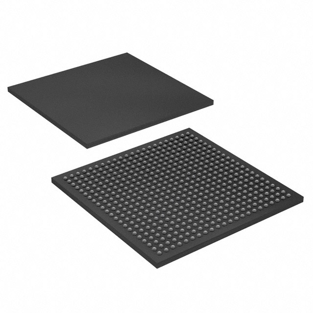
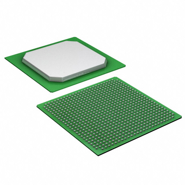
EP2C35F672C8
| Part Description |
Cyclone® II Field Programmable Gate Array (FPGA) IC 475 483840 33216 672-BGA |
|---|---|
| Quantity | 452 Available (as of June 14, 2026) |

| Product Category | Field Programmable Gate Array (FPGA) |
|---|---|
| Manufacturer | Intel |
| Manufacturing Status | Active |
| Manufacturer Standard Lead Time | 8 Weeks |
| Datasheet |
Specifications & Environmental
| Device Package | 672-FBGA (27x27) | Grade | Commercial | Operating Temperature | 0°C – 85°C | ||
|---|---|---|---|---|---|---|---|
| Package / Case | 672-BGA | Number of I/O | 475 | Voltage | 1.15 V - 1.25 V | ||
| Mounting Method | Surface Mount | RoHS Compliance | RoHS non-compliant | REACH Compliance | REACH Unaffected | ||
| Moisture Sensitivity Level | 3 (168 Hours) | Number of LABs/CLBs | 2076 | Number of Logic Elements/Cells | 33216 | ||
| Number of Gates | N/A | ECCN | 3A991D | HTS Code | 8542.39.0001 | ||
| Qualification | N/A | Total RAM Bits | 483840 |
Overview of EP2C35F672C8 – Cyclone® II Field Programmable Gate Array (FPGA) IC 475 483840 33216 672-BGA
The EP2C35F672C8 is an Intel Cyclone® II FPGA in a 672-ball BGA package, designed for low-cost embedded processing and DSP-oriented solutions. The device integrates a dense logic fabric with on-chip memory and extensive I/O to support complex control, interfacing, and signal-processing tasks in commercial applications.
Key elements include 33,216 logic elements, approximately 0.48 Mbits of embedded memory, and 475 general-purpose I/Os, all in a surface-mount 672-FBGA (27×27) package. The device operates over a 1.15 V to 1.25 V core voltage range and is specified for 0 °C to 85 °C commercial use.
Key Features
- Core Logic 33,216 logic elements provide substantial programmable logic capacity for glue logic, state machines, and custom datapaths.
- Logic Array Blocks (LABs) 2,076 LABs (Logic Array Blocks) for organized routing and placement of logic resources across the device.
- Embedded Memory Approximately 0.48 Mbits of on-chip RAM to implement FIFOs, buffers, and small data stores close to logic.
- I/O Count 475 I/O pins support high-density interfacing to peripherals, sensors, and external memory devices.
- On-Chip Clocking Cyclone II device family features a global clock network and phase-locked loop (PLL) architecture for flexible clock distribution and management.
- Voltage and Power Core supply specified from 1.15 V to 1.25 V, enabling designs targeting the Cyclone II core-voltage envelope.
- Package & Mounting Surface-mount 672-BGA footprint; supplier package listed as 672-FBGA (27×27), offering a compact high-pin-count solution.
- Operating Range & Compliance Commercial-grade operating temperature of 0 °C to 85 °C and RoHS-compliant construction.
Typical Applications
- Low-Cost Embedded Processing Implement microcontroller-style hardware accelerators, control logic, and custom I/O management within cost-sensitive systems.
- Low-Cost DSP Solutions Deploy signal-processing blocks and datapaths using on-chip logic and embedded memory for audio, communications, or sensor processing tasks.
- External Memory Interfacing Use the abundant I/O and dedicated interfacing resources to connect to external memory and high-speed peripherals.
- High-Density I/O Control Drive systems requiring many parallel inputs and outputs such as board-level protocol bridging, display control, and multi-channel data aggregation.
Unique Advantages
- Substantial Logic Capacity: 33,216 logic elements enable complex finite-state machines and custom hardware accelerators without external glue logic.
- Integrated Memory: Approximately 0.48 Mbits of embedded RAM reduces reliance on external RAM for small buffers and FIFOs, simplifying board design.
- High I/O Density: 475 I/Os allow flexible, parallel interfacing to a wide range of peripherals and external devices, minimizing the need for additional I/O expanders.
- Family-Level Clocking Features: Built-in global clock network and PLL architecture (Cyclone II family) provide flexible clock distribution for synchronous designs.
- Compact Package: 672-FBGA (27×27) surface-mount package delivers high pin count in a compact footprint for space-constrained boards.
- Commercial-Grade and RoHS-Compliant: Rated 0 °C to 85 °C and RoHS-compliant to meet commercial manufacturing and regulatory expectations.
Why Choose EP2C35F672C8?
The EP2C35F672C8 positions itself as a practical Cyclone II FPGA choice for designers who need substantial programmable logic, embedded memory, and large I/O capacity in a compact BGA package. Its combination of 33,216 logic elements, approximately 0.48 Mbits of on-chip RAM, and 475 I/Os supports a wide range of commercial embedded and DSP-oriented designs.
This device is well suited to teams building cost-sensitive systems that require integrated logic and memory, predictable operating conditions (1.15 V–1.25 V core, 0 °C–85 °C), and RoHS-compliant manufacturing. The Cyclone II family’s documented architecture and clocking features provide a stable platform for development and deployment.
Request a quote or submit an inquiry to get pricing and availability for the EP2C35F672C8 and include your quantity and delivery requirements for a prompt response.


Date Founded: 1968
Headquarters: Santa Clara, California, USA
Employees: 130,000+
Revenue: $54.23 Billion
Certifications and Memberships: ISO9001:2015, ISO14001:2015, ISO17025:2017, ISO27001:2022, ISO45001:2018, ISO50001:2018


