
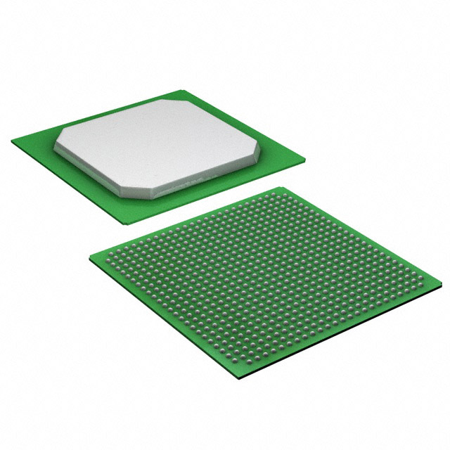
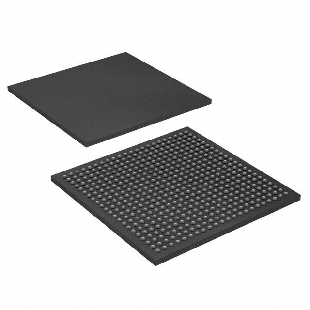
EP2C35F672C8N
| Part Description |
Cyclone® II Field Programmable Gate Array (FPGA) IC 475 483840 33216 672-BGA |
|---|---|
| Quantity | 385 Available (as of June 15, 2026) |
| Product Category | Field Programmable Gate Array (FPGA) |
|---|---|
| Manufacturer | Intel |
| Manufacturing Status | Active |
| Manufacturer Standard Lead Time | 26 Weeks |
| Datasheet |
Specifications & Environmental
| Device Package | 672-FBGA (27x27) | Grade | Commercial | Operating Temperature | 0°C – 85°C | ||
|---|---|---|---|---|---|---|---|
| Package / Case | 672-BGA | Number of I/O | 475 | Voltage | 1.15 V - 1.25 V | ||
| Mounting Method | Surface Mount | RoHS Compliance | RoHS Compliant | REACH Compliance | REACH Unaffected | ||
| Moisture Sensitivity Level | 3 (168 Hours) | Number of LABs/CLBs | 2076 | Number of Logic Elements/Cells | 33216 | ||
| Number of Gates | N/A | ECCN | 3A991D | HTS Code | 8542.39.0001 | ||
| Qualification | N/A | Total RAM Bits | 483840 |
Overview of EP2C35F672C8N – Cyclone® II FPGA, 33,216 logic elements, 672-FBGA
The EP2C35F672C8N is a Cyclone® II field-programmable gate array (FPGA) in a 672‑FBGA package. It implements the Cyclone II architecture with a substantial logic fabric and embedded on-chip memory, targeting low-cost embedded processing and DSP-oriented applications.
With 475 I/O pins, support for programmable I/O features, integrated multipliers and PLLs, and a compact surface-mount 27×27 672‑FBGA package, this device is intended for designers needing dense I/O, flexible clocking and embedded memory in commercial-temperature systems.
Key Features
- Logic Fabric — 33,216 logic elements and 2,076 logic array blocks provide the programmable logic resources for custom control, interface and compute functions.
- Embedded Memory — Approximately 0.48 Mbits (483,840 bits) of on-chip RAM implemented with M4K memory blocks for packet buffering, FIFO storage and small on-chip data structures.
- DSP and Clocking — Integrated embedded multipliers and phase-locked loops (PLLs) enable basic DSP operations and flexible clock management for synchronous designs.
- I/O Capacity & Flexibility — 475 user I/O pins with support for advanced I/O standards, differential interfaces, programmable drive strength, slew-rate control and on-chip series termination for robust external interfacing.
- Package & Mounting — Supplied in a 672‑FBGA (27×27) surface-mount package for high-density board layouts and reliable soldered mounting.
- Power & Environmental — Core supply range 1.15 V to 1.25 V and commercial operating temperature range of 0 °C to 85 °C; RoHS compliant.
- Configuration & Test Support — Includes IEEE 1149.1 (JTAG) boundary-scan support and multiple configuration schemes for device programming and board-level testability.
Typical Applications
- Embedded Processing — Implement microcontroller-like peripherals, custom state machines and control logic for low-cost embedded systems.
- DSP Functions — Use the device’s embedded multipliers and on-chip memory for basic digital signal processing tasks, filtering and data path acceleration.
- High-Density I/O Systems — Interfaces requiring many parallel signals or differential pairs benefit from the 475 I/O pins and programmable I/O features.
- External Memory Interfaces — Support for external memory interfacing makes this FPGA suitable for designs that combine on-chip resources with off-chip RAM or flash.
Unique Advantages
- High logic capacity: 33,216 logic elements and 2,076 logic array blocks give designers room to implement complex control and processing functions on a single device.
- Significant on-chip RAM: Approximately 0.48 Mbits of embedded memory reduces dependence on external memory for small to moderate data buffering and state storage.
- Extensive I/O resources: 475 I/O pins with advanced I/O features simplify board-level connectivity and support a wide range of interface standards.
- Flexible clocking and DSP support: Integrated PLLs and embedded multipliers enable practical clock management and arithmetic acceleration within the FPGA fabric.
- Compact, surface-mount package: The 672‑FBGA (27×27) package allows dense PCBs while maintaining robust soldered connections for production assemblies.
- Commercial-grade operation and compliance: Designed for 0 °C to 85 °C operation and RoHS compliant for standard commercial applications and manufacturing.
Why Choose EP2C35F672C8N?
The EP2C35F672C8N blends substantial programmable logic, embedded memory and DSP-oriented resources with a high I/O count in a compact 672‑FBGA package. It is positioned for commercial designs that require flexible interfacing, on-chip buffering and configurable signal processing within a Cyclone II architecture.
This device is well suited to engineers developing embedded processing platforms, DSP-accelerated subsystems and I/O-intensive controllers who value a balance of integration, configurability and board-level density backed by the Cyclone II device family documentation and feature set.
Request a quote or submit a pricing inquiry to check availability and receive ordering information for EP2C35F672C8N.


Date Founded: 1968
Headquarters: Santa Clara, California, USA
Employees: 130,000+
Revenue: $54.23 Billion
Certifications and Memberships: ISO9001:2015, ISO14001:2015, ISO17025:2017, ISO27001:2022, ISO45001:2018, ISO50001:2018


