
EP2C35U484C6
| Part Description |
Cyclone® II Field Programmable Gate Array (FPGA) IC 322 483840 33216 484-FBGA |
|---|---|
| Quantity | 1,990 Available (as of June 14, 2026) |

| Product Category | Field Programmable Gate Array (FPGA) |
|---|---|
| Manufacturer | Intel |
| Manufacturing Status | Active |
| Manufacturer Standard Lead Time | 26 Weeks |
| Datasheet |
Specifications & Environmental
| Device Package | 484-UBGA (19x19) | Grade | Commercial | Operating Temperature | 0°C – 85°C | ||
|---|---|---|---|---|---|---|---|
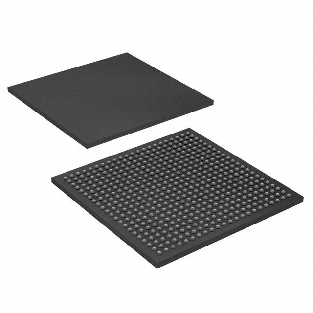
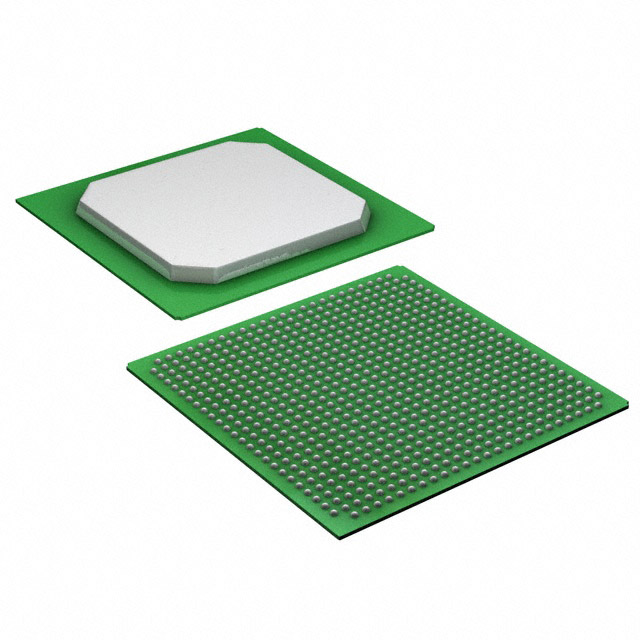
| Package / Case | 484-FBGA | Number of I/O | 322 | Voltage | 1.15 V - 1.25 V | ||
| Mounting Method | Surface Mount | RoHS Compliance | RoHS non-compliant | REACH Compliance | REACH Unaffected | ||
| Moisture Sensitivity Level | 3 (168 Hours) | Number of LABs/CLBs | 2076 | Number of Logic Elements/Cells | 33216 | ||
| Number of Gates | N/A | ECCN | 3A991D | HTS Code | 8542.39.0001 | ||
| Qualification | N/A | Total RAM Bits | 483840 |
Overview of EP2C35U484C6 – Cyclone® II Field Programmable Gate Array (FPGA) IC 322 483840 33216 484-FBGA
The EP2C35U484C6 is a Cyclone® II family FPGA from Intel offered in a 484‑FBGA (484‑UBGA 19×19) surface‑mount package. It implements the Cyclone II architecture with dedicated clock circuitry, embedded memory, and programmable I/O to address a range of low‑cost embedded processing and DSP applications.
With 33,216 logic elements, approximately 0.48 Mbits of on‑chip RAM and 322 available I/O pins, this commercial‑grade device targets designs that require moderate logic density, flexible I/O capability, and a compact board footprint while operating within a 1.15 V–1.25 V supply range and 0 °C–85 °C temperature window.
Key Features
- Logic Capacity — 33,216 logic elements and 2,076 LABs provide substantial programmable logic for glue logic, state machines, and custom datapaths.
- Embedded Memory — Approximately 0.48 Mbits of on‑chip RAM for FIFOs, buffers and small on‑chip storage requirements.
- I/O Resources — 322 user I/Os in a multi‑bank architecture to support diverse interface needs and board routing strategies.
- Cyclone II Architecture — Family architecture with global clock networks, PLLs, embedded multipliers and documented memory modes for common FPGA system tasks.
- I/O Features — Device handbook references support for programmable drive strength, series on‑chip termination, slew rate control and a broad set of I/O standards and differential interfaces.
- Power — Core voltage supply range of 1.15 V to 1.25 V to match system power domains and enable predictable power planning.
- Package & Mounting — 484‑FBGA (484‑UBGA, 19×19) surface‑mount package for compact, high‑density board designs.
- Commercial Temperature & RoHS — Rated for 0 °C to 85 °C operation and RoHS compliant for standard commercial applications.
Typical Applications
- Low‑Cost Embedded Processing — Implement microcontroller offload, protocol handling and glue logic in compact embedded systems.
- Digital Signal Processing (DSP) — Use embedded multipliers and on‑chip RAM for moderate DSP tasks, filters and data path acceleration.
- Interface Bridging — Support diverse parallel and differential interfaces using the device’s large I/O count and programmable I/O features.
- Prototyping & Proof‑of‑Concept — Provide a cost‑effective platform for developing and validating custom logic and system prototypes.
Unique Advantages
- High logic density for the package: 33,216 logic elements deliver significant programmable logic in a 484‑FBGA footprint, helping reduce board count and simplify designs.
- Substantial on‑chip RAM: Approximately 0.48 Mbits of embedded memory reduces the need for external RAM in many buffering and storage use cases.
- Extensive I/O flexibility: 322 I/Os and Cyclone II I/O features (programmable drive strength, on‑chip termination, differential support) enable diverse peripheral and memory interfaces.
- Clocking and timing resources: Family architecture includes global clock networks and PLLs to manage multiple clock domains and timing requirements.
- Compact, surface‑mount package: The 484‑FBGA (19×19) package supports high‑density board layouts for space‑constrained applications.
- Commercial‑grade reliability: Rated for 0 °C to 85 °C operation and RoHS compliant for standard commercial product environments.
Why Choose EP2C35U484C6?
The EP2C35U484C6 delivers a balanced combination of programmable logic capacity, embedded memory and a broad I/O set within a compact 484‑FBGA package. It is well suited for engineers seeking a Cyclone II family device for low‑cost embedded processing, moderate DSP acceleration and flexible interface integration in commercial temperature environments.
Designed around the Cyclone II architecture and supported by family documentation covering logic elements, global clocking, PLLs, embedded memory modes and I/O features, this device provides a clear, verifiable specification set for predictable system integration and BOM planning.
Request a quote or submit an inquiry to receive pricing and availability information for EP2C35U484C6.


Date Founded: 1968
Headquarters: Santa Clara, California, USA
Employees: 130,000+
Revenue: $54.23 Billion
Certifications and Memberships: ISO9001:2015, ISO14001:2015, ISO17025:2017, ISO27001:2022, ISO45001:2018, ISO50001:2018


