
EP4SE820F43C3
| Part Description |
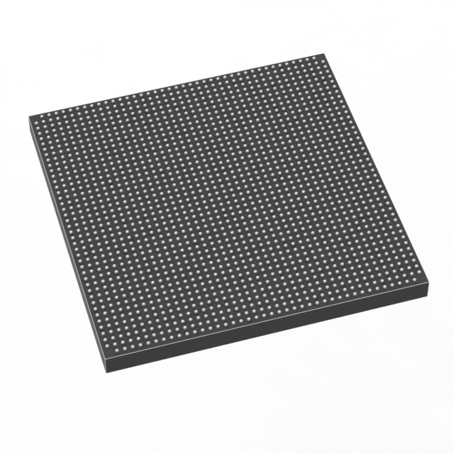
STRATIX® IV E Field Programmable Gate Array (FPGA) IC 1120 34093056 813050 1760-BBGA, FCBGA |
|---|---|
| Quantity | 1,784 Available (as of June 14, 2026) |

| Product Category | Field Programmable Gate Array (FPGA) |
|---|---|
| Manufacturer | Intel |
| Manufacturing Status | Obsolete |
| Manufacturer Standard Lead Time | Contact Us |
| Datasheet |
Specifications & Environmental
| Device Package | 1760-FCBGA (42.5x42.5) | Grade | Commercial | Operating Temperature | 0°C – 85°C | ||
|---|---|---|---|---|---|---|---|
| Package / Case | 1760-BBGA, FCBGA | Number of I/O | 1120 | Voltage | 870 mV - 930 mV | ||
| Mounting Method | Surface Mount | RoHS Compliance | RoHS non-compliant | REACH Compliance | REACH Unknown | ||
| Moisture Sensitivity Level | 3 (168 Hours) | Number of LABs/CLBs | 32522 | Number of Logic Elements/Cells | 813050 | ||
| Number of Gates | N/A | ECCN | 3A001A7A | HTS Code | 8542.39.0001 | ||
| Qualification | N/A | Total RAM Bits | 34093056 |
Overview of EP4SE820F43C3 – STRATIX® IV E Field Programmable Gate Array (FPGA) IC, 1760‑FCBGA (42.5×42.5)
The EP4SE820F43C3 is a Stratix IV E family FPGA from Intel, offered as a high-density, commercial-grade Field Programmable Gate Array in a 1760‑FBGA surface‑mount package. It delivers a large logic fabric and on‑chip memory alongside extensive I/O to address demanding digital design requirements.
This device is aimed at applications that require high logic capacity, significant embedded memory and large I/O counts. Key value propositions include high logic density, substantial embedded RAM, low-voltage core operation range and a high‑pin‑count FCBGA package for complex system integration.
Key Features
- Logic Capacity Approximately 813,050 logic elements, enabling large, complex designs.
- Logic Array Blocks 32,522 logic blocks (as provided in device specifications) to structure the on‑chip logic fabric.
- Embedded Memory Approximately 34 Mbits of embedded memory (34,093,056 total RAM bits) for buffering, FIFOs and on‑chip storage.
- I/O Density 1,120 user I/Os to support multiple parallel interfaces and complex board‑level connectivity.
- Core Supply Voltage Low‑voltage core operation from 870 mV to 930 mV to align with modern low‑power design targets.
- Package and Mounting 1760‑BBGA / 1760‑FCBGA surface‑mount package (42.5×42.5 mm) for high pin count and board‑level integration.
- Temperature and Grade Commercial grade with an operating temperature range of 0 °C to 85 °C.
- Architecture Features Device handbook details for the Stratix IV family include embedded memory, DSP blocks, clock networks and PLLs, high‑speed transceiver features, and support for external memory interfaces.
- Compliance RoHS compliant.
Typical Applications
- High‑performance data processing Large logic capacity and substantial embedded memory provide on‑chip resources for compute‑intensive signal processing and data manipulation.
- High‑pin‑count interface aggregation 1,120 I/Os accommodate dense parallel interfaces, board‑level aggregation and complex I/O routing.
- External memory controller and bridging Architectural support for external memory interfaces makes the device suitable for designs that require on‑board DRAM or other off‑chip storage management.
- Digital signal processing (DSP) The device family documentation cites DSP blocks and clocking resources appropriate for DSP pipelines and real‑time processing tasks.
Unique Advantages
- High logic density: ~813,050 logic elements allow integration of large functions and complex state machines on a single device, reducing board count.
- Significant on‑chip RAM: Approximately 34 Mbits of embedded memory reduces dependence on external memory for buffering and data staging.
- Extensive I/O resources: 1,120 I/Os enable broad external connectivity without multiple interface chips.
- Low‑voltage core operation: 870–930 mV supply range supports modern power‑optimized system designs.
- High‑density package: 1760‑FCBGA 42.5×42.5 mm package supports high pin counts in a surface‑mount form factor for compact system layouts.
- Standards‑oriented architecture: Stratix IV E family documentation references features such as PLLs, clock networks, DSP blocks and high‑speed transceiver capabilities to support protocol and bandwidth requirements.
Why Choose EP4SE820F43C3?
The EP4SE820F43C3 is positioned for designers who require a high‑density Stratix IV E FPGA with substantial embedded memory, a large I/O set and a high‑pin‑count FCBGA package. Its combination of ~813k logic elements, approximately 34 Mbits of on‑chip RAM and 1,120 I/Os supports complex integration, high‑channel counts and data‑intensive processing within a commercial‑grade operating range.
As a member of Intel’s Stratix IV E family and provided as a RoHS‑compliant, surface‑mount 1760‑FCBGA device, it is suitable for mainstream electronic applications that demand scalable logic capacity, robust on‑chip memory resources and comprehensive I/O for board‑level system design.
Request a quote or submit an inquiry to get pricing and availability for EP4SE820F43C3.


Date Founded: 1968
Headquarters: Santa Clara, California, USA
Employees: 130,000+
Revenue: $54.23 Billion
Certifications and Memberships: ISO9001:2015, ISO14001:2015, ISO17025:2017, ISO27001:2022, ISO45001:2018, ISO50001:2018


