
EP4SE820F43C3G
| Part Description |
Field Programmable Gate Array (FPGA) IC |
|---|---|
| Quantity | 527 Available (as of June 10, 2026) |
| Product Category | Field Programmable Gate Array (FPGA) |
|---|---|
| Manufacturer | Intel |
| Manufacturing Status | Active |
| Manufacturer Standard Lead Time | 8 Weeks |
| Datasheet |
Specifications & Environmental
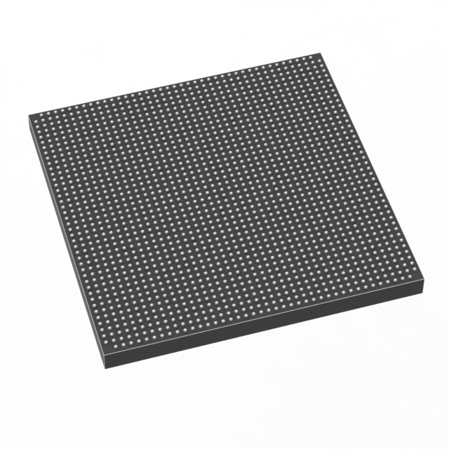
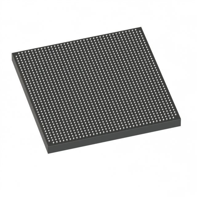
| Device Package | 1760-FCBGA (42.5x42.5) | Grade | Commercial | Operating Temperature | 0°C – 85°C | ||
|---|---|---|---|---|---|---|---|
| Package / Case | 1760-BBGA, FCBGA | Number of I/O | 1120 | Voltage | 870 mV - 930 mV | ||
| Mounting Method | Surface Mount | RoHS Compliance | RoHS Compliant | REACH Compliance | REACH Unaffected | ||
| Moisture Sensitivity Level | 3 (168 Hours) | Number of LABs/CLBs | 32522 | Number of Logic Elements/Cells | 813050 | ||
| Number of Gates | N/A | ECCN | N/A | HTS Code | N/A | ||
| Qualification | N/A | Total RAM Bits | 34093056 |
Overview of EP4SE820F43C3G – Field Programmable Gate Array (FPGA) IC
The EP4SE820F43C3G is a commercial‑grade Field Programmable Gate Array (FPGA) IC from Intel, based on the Stratix IV device family. It delivers a large logic fabric and on‑chip memory in a high‑density FCBGA package for demanding digital designs.
With approximately 813,050 logic elements and roughly 34 Mbits of embedded memory, the device targets high‑capacity integration where extensive I/O (1,120 pins) and high aggregate data bandwidth are required. The device operates from a core supply of 870 mV to 930 mV and is specified for 0 °C to 85 °C operation.
Key Features
- Logic Capacity Approximately 813,050 logic elements provide large combinational and sequential resource density for complex FPGA designs.
- Fabric Scale Large fabric scale reflected by 32,522 fabric blocks, enabling partitioned designs and high logic utilization.
- Embedded Memory Approximately 34 Mbits of embedded memory for on‑chip buffering, lookup tables and state storage.
- High I/O Count 1,120 I/O pins accommodate broad connectivity to external devices, memories, and system interfaces.
- Stratix IV Family Architecture Series features documented in the Stratix IV Device Handbook include dedicated DSP blocks, PLLs, clock networks, high‑speed transceiver features and external memory interface support.
- Power and Voltage Core voltage specified between 870 mV and 930 mV to match system power-rail requirements for the device core.
- Package and Mounting 1760‑ball FCBGA (1760‑BBGA) supplier package, 42.5 × 42.5 mm footprint; surface‑mount mounting for compact board integration.
- Operational Grade and Temperature Commercial grade device rated for operation from 0 °C to 85 °C.
- Regulatory RoHS compliant.
Typical Applications
- High‑bandwidth Data Processing Large logic and embedded memory support parallel data paths and custom data‑plane processing required in high‑throughput designs.
- Networking and Telecom Stratix IV family transceiver and protocol features suit packet processing, protocol bridging and line‑rate logic implementations.
- Video and Signal Processing Abundant logic and on‑chip memory enable frame buffering, filtering and real‑time signal chains.
- Memory Interface and Bridge Logic High I/O count and documented external memory interface support facilitate complex memory controllers and interface bridging.
Unique Advantages
- High Logic Density: Approximately 813,050 logic elements allow integration of large, multi‑function designs on a single device, reducing board‑level complexity.
- Substantial On‑Chip Memory: About 34 Mbits of embedded RAM supports on‑chip data buffering and state storage without immediate dependence on external memory.
- Extensive I/O Resources: 1,120 I/O pins provide flexible connectivity for parallel buses, high‑speed interfaces and multiple peripherals.
- Stratix IV Architecture: Family features such as DSP blocks, PLLs and high‑speed transceivers (as documented in the Stratix IV Device Handbook) enable implementation of performance‑oriented functions.
- Compact FCBGA Packaging: 1760‑ball FCBGA package (42.5 × 42.5 mm) offers a high‑pin‑count solution with a surface‑mount footprint suitable for dense system designs.
- Commercial Temperature and RoHS Compliance: Rated for 0 °C to 85 °C operation and RoHS‑compliant for standard commercial applications.
Why Choose EP4SE820F43C3G?
EP4SE820F43C3G combines substantial logic capacity, significant embedded memory and a very high I/O count in a Stratix IV‑family FPGA package, making it appropriate for complex, high‑integration digital systems. Its documented family features—DSP resources, clocking and transceiver support—align with demanding data‑path and protocol applications.
Designed for commercial deployments, the device delivers a balance of performance, integration and proven family architecture for teams building high‑capacity processing, networking, video or memory‑interface solutions backed by the Stratix IV device documentation.
Request a quote or submit an inquiry to receive pricing and availability for EP4SE820F43C3G.


Date Founded: 1968
Headquarters: Santa Clara, California, USA
Employees: 130,000+
Revenue: $54.23 Billion
Certifications and Memberships: ISO9001:2015, ISO14001:2015, ISO17025:2017, ISO27001:2022, ISO45001:2018, ISO50001:2018


