
EP4SE820F43I4G
| Part Description |
Field Programmable Gate Array (FPGA) IC |
|---|---|
| Quantity | 389 Available (as of October 7, 2026) |

| Product Category | Field Programmable Gate Array (FPGA) |
|---|---|
| Manufacturer | Intel |
| Manufacturing Status | Active |
| Manufacturer Standard Lead Time | 8 Weeks |
| Datasheet |
Specifications & Environmental
| Device Package | 1760-FCBGA (42.5x42.5) | Grade | Industrial | Operating Temperature | -40°C – 100°C | ||
|---|---|---|---|---|---|---|---|
| Package / Case | 1760-BBGA, FCBGA | Number of I/O | 1120 | Voltage | 870 mV - 930 mV | ||
| Mounting Method | Surface Mount | RoHS Compliance | RoHS Compliant | REACH Compliance | REACH Unaffected | ||
| Moisture Sensitivity Level | 3 (168 Hours) | Number of LABs/CLBs | 32522 | Number of Logic Elements/Cells | 813050 | ||
| Number of Gates | N/A | ECCN | N/A | HTS Code | N/A | ||
| Qualification | N/A | Total RAM Bits | 34093056 |
Overview of EP4SE820F43I4G – Field Programmable Gate Array (FPGA) IC
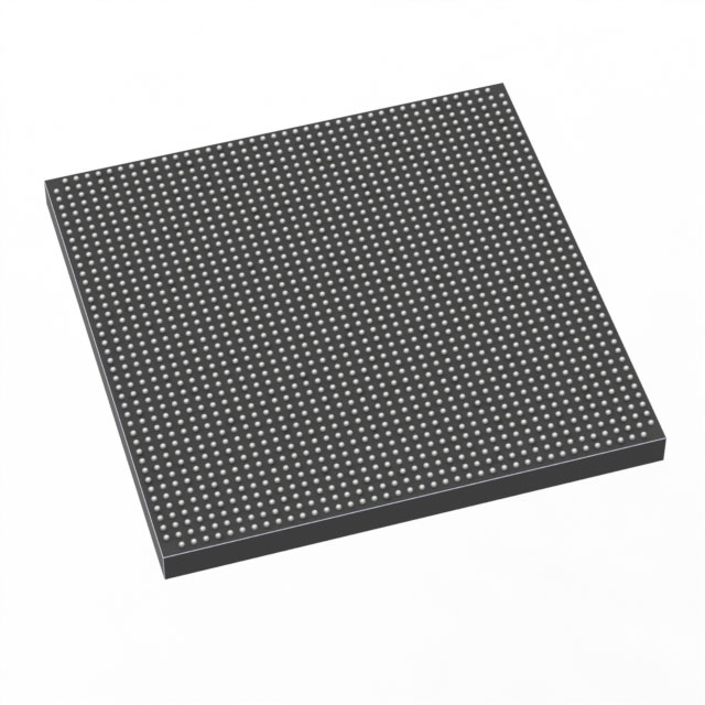
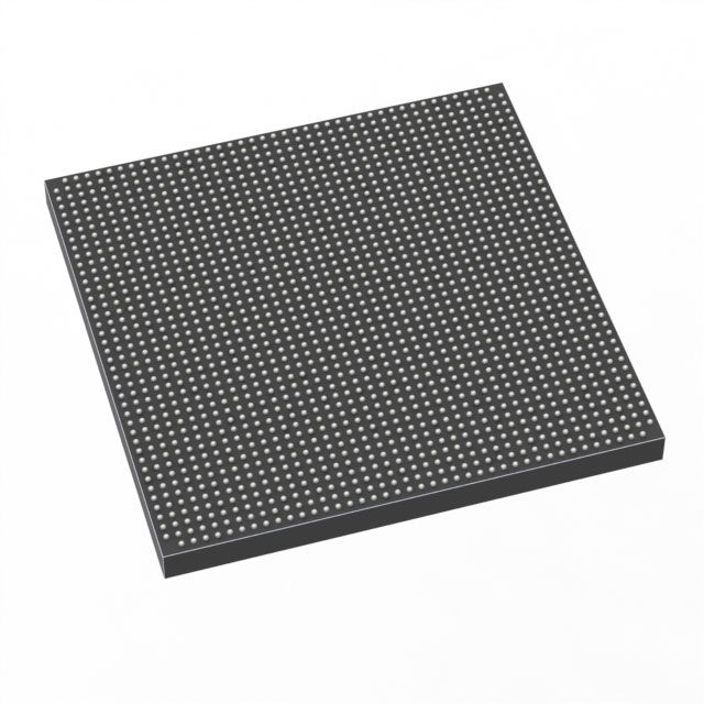
The EP4SE820F43I4G is an Intel Stratix IV family FPGA in a 1760‑pin FCBGA package, designed for dense, high‑pin‑count programmable logic implementations. It delivers a large logic capacity, substantial embedded memory, and broad I/O to support complex digital designs in industrial applications.
Key attributes include approximately 813,050 logic elements, roughly 34 Mbits of embedded memory, 1,120 I/O, a 1760‑FCBGA (42.5×42.5 mm) package with surface‑mount mounting, and industrial operating range from −40 °C to 100 °C. Device documentation is provided in the Stratix IV Device Handbook referenced in the product datasheet.
Key Features
- Core Capacity Approximately 813,050 logic elements for implementing large, complex FPGA designs.
- Embedded Memory Approximately 34 Mbits of on‑chip RAM to support data buffering, tables, and local storage for logic functions.
- I/O Density 1,120 I/O pins to interface with multiple high‑pin‑count peripherals and system buses.
- Package & Mounting 1760‑FCBGA (42.5 × 42.5 mm) package, 1760‑BBGA footprint variant; designed for surface‑mount assembly.
- Power Supply Range Core supply specified between 870 mV and 930 mV for targeted power domains.
- Industrial Temperature Grade Rated for operation from −40 °C to 100 °C for deployments in industrial environments.
- System & Clock Architecture (Series) The Stratix IV device handbook documents clock networks and PLL resources typical of the family, offering design guidance for clocking and timing architectures.
- Standards & Compliance RoHS compliant as indicated in the product data.
Typical Applications
- High‑performance networking and switching Leverage the high logic density and large I/O count for packet processing, protocol handling, and interface aggregation.
- Telecommunications infrastructure Use embedded memory and the Stratix IV family device features for buffering, framing, and timing functions in telecom equipment.
- Data acquisition and processing Implement wide parallel data paths and local memory for real‑time capture, aggregation, and preprocessing.
- High‑pin‑count system controllers Integrate multiple subsystems and external memories using the extensive I/O resources and large logic capacity.
Unique Advantages
- High logic density: The device provides approximately 813,050 logic elements, enabling integration of large custom logic blocks on a single FPGA.
- Significant on‑chip memory: Approximately 34 Mbits of embedded memory reduces dependence on external RAM for many buffering and storage tasks.
- Large I/O complement: 1,120 I/O pins support multiple parallel interfaces and high‑pin‑count subsystem connections, simplifying board‑level routing for complex systems.
- Industrial temperature capability: Rated from −40 °C to 100 °C for reliable operation in industrial environments and extended temperature applications.
- Compact, assembly‑ready package: 1760‑FCBGA (42.5 × 42.5 mm) in a surface‑mount format for high‑density PCB integration.
- Documented architecture: The Stratix IV Device Handbook provides reference material on device core features, clock networks, PLLs, transceiver and I/O capabilities to support system design and validation.
Why Choose EP4SE820F43I4G?
The EP4SE820F43I4G positions itself for designs that require substantial programmable logic, significant embedded memory, and a high I/O count in an industrial‑grade package. Its specification set addresses complex digital signal processing, high‑throughput interfacing, and multi‑interface system control where integration density and temperature robustness matter.
Designers and system integrators targeting scalable, long‑lifecycle deployments will find the combination of logic capacity, on‑chip memory, and comprehensive device documentation useful for developing and validating sophisticated FPGA‑based solutions.
Request a quote or contact our sales team to discuss availability, lead times, and pricing for the EP4SE820F43I4G. Provide your project requirements and quantity for a tailored response.


























Date Founded: 1968
Headquarters: Santa Clara, California, USA
Employees: 130,000+
Revenue: $54.23 Billion
Certifications and Memberships: ISO9001:2015, ISO14001:2015, ISO17025:2017, ISO27001:2022, ISO45001:2018, ISO50001:2018


