
EP4SGX290FF35C2XN
| Part Description |
Stratix® IV GX Field Programmable Gate Array (FPGA) IC 564 17661952 291200 1152-BBGA, FCBGA |
|---|---|
| Quantity | 1,148 Available (as of June 14, 2026) |

| Product Category | Field Programmable Gate Array (FPGA) |
|---|---|
| Manufacturer | Intel |
| Manufacturing Status | Obsolete |
| Manufacturer Standard Lead Time | Contact Us |
| Datasheet |
Specifications & Environmental
| Device Package | 1152-FBGA (35x35) | Grade | Commercial | Operating Temperature | 0°C – 85°C | ||
|---|---|---|---|---|---|---|---|
| Package / Case | 1152-BBGA, FCBGA | Number of I/O | 564 | Voltage | 870 mV - 930 mV | ||
| Mounting Method | Surface Mount | RoHS Compliance | RoHS Compliant | REACH Compliance | REACH Unknown | ||
| Moisture Sensitivity Level | 3 (168 Hours) | Number of LABs/CLBs | 11648 | Number of Logic Elements/Cells | 291200 | ||
| Number of Gates | N/A | ECCN | 3A001A7A | HTS Code | 8542.39.0001 | ||
| Qualification | N/A | Total RAM Bits | 17661952 |
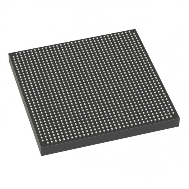
Overview of EP4SGX290FF35C2XN – Stratix® IV GX FPGA, 291,200 logic elements, 1152‑FBGA
The EP4SGX290FF35C2XN is a Stratix IV GX Field Programmable Gate Array (FPGA) delivered in a 1152‑FBGA (35×35) surface‑mount package. It provides a high‑capacity programmable fabric with 291,200 logic elements, approximately 16.8 Mbits of embedded memory, and 564 I/O pins for complex system integration.
Designed for applications that require large logic capacity, extensive on‑chip memory and substantial I/O, this commercial‑grade device operates from 0 °C to 85 °C and is RoHS compliant. It is built on the Stratix IV GX device family architecture, which includes high‑speed transceiver support, DSP capabilities, PLLs and advanced clocking as described in the device handbook.
Key Features
- Core Logic 291,200 logic elements provide the programmable fabric needed for large FPGA designs and complex logic implementation.
- Embedded Memory Approximately 16.8 Mbits of on‑chip RAM to support large buffers, FIFOs and local data storage without external memory.
- I/O Capacity 564 I/O pins enable dense connectivity for parallel interfaces, external memory buses and multiple high‑speed links.
- Stratix IV GX Architecture Device family features include high‑speed transceivers, digital signal processing (DSP) blocks, PLLs and advanced clock networks as documented in the Stratix IV device handbook.
- Power and Supply Core supply operating range of 0.870 V to 0.930 V for the device core domain.
- Package and Mounting 1152‑BBGA / 1152‑FBGA (35×35) ball‑grid package, surface‑mount for high‑density PCB integration.
- Commercial Temperature Grade Rated for 0 °C to 85 °C operation to meet standard commercial application environments.
- Compliance RoHS compliant for environmental and regulatory conformity.
Typical Applications
- High‑speed communications Leverages the Stratix IV GX architecture’s transceiver and I/O capacity to implement protocol stacks and high‑bandwidth links.
- Signal processing and DSP Large logic capacity and on‑chip memory support complex DSP pipelines and real‑time data manipulation.
- Networking and data aggregation Extensive I/O and embedded memory allow packet buffering, bridging and aggregation functions in network equipment.
- Custom compute and accelerator functions High logic density and DSP resources enable implementation of hardware accelerators and application‑specific processing engines.
Unique Advantages
- High programmable capacity: 291,200 logic elements provide headroom for complex designs and feature integration on a single device.
- Substantial on‑chip memory: Approximately 16.8 Mbits of embedded RAM reduces dependence on external memory for buffering and local storage.
- Extensive I/O count: 564 I/O pins simplify board‑level routing for multi‑interface designs and parallel data paths.
- Stratix IV GX family features: Architecture includes high‑speed transceivers, DSP blocks, PLLs and advanced clock networks as documented in the device handbook, enabling protocol and timing flexibility.
- Compact, manufacturable package: 1152‑FBGA (35×35) surface‑mount package supports high‑density PCB layouts while meeting assembly standards.
- Commercial grade and compliant: 0 °C to 85 °C operating range and RoHS compliance align with standard commercial product requirements.
Why Choose EP4SGX290FF35C2XN?
The EP4SGX290FF35C2XN combines large FPGA fabric, significant embedded memory and extensive I/O in a single 1152‑FBGA package, making it well suited for high‑complexity designs that require high logic capacity and on‑chip resources. Its Stratix IV GX family architecture provides the system‑level building blocks — including transceiver and DSP capabilities — documented in the device handbook.
This part is aimed at designers and teams building communication systems, signal processing platforms, networking equipment and custom compute accelerators who need a high‑capacity, commercial‑grade FPGA with verified device‑family features and RoHS compliance.
Request a quote or submit an inquiry to purchase the EP4SGX290FF35C2XN and evaluate how its capacity, memory and I/O resources can simplify your next design.


Date Founded: 1968
Headquarters: Santa Clara, California, USA
Employees: 130,000+
Revenue: $54.23 Billion
Certifications and Memberships: ISO9001:2015, ISO14001:2015, ISO17025:2017, ISO27001:2022, ISO45001:2018, ISO50001:2018


