
EP4SGX290HF35C2N
| Part Description |
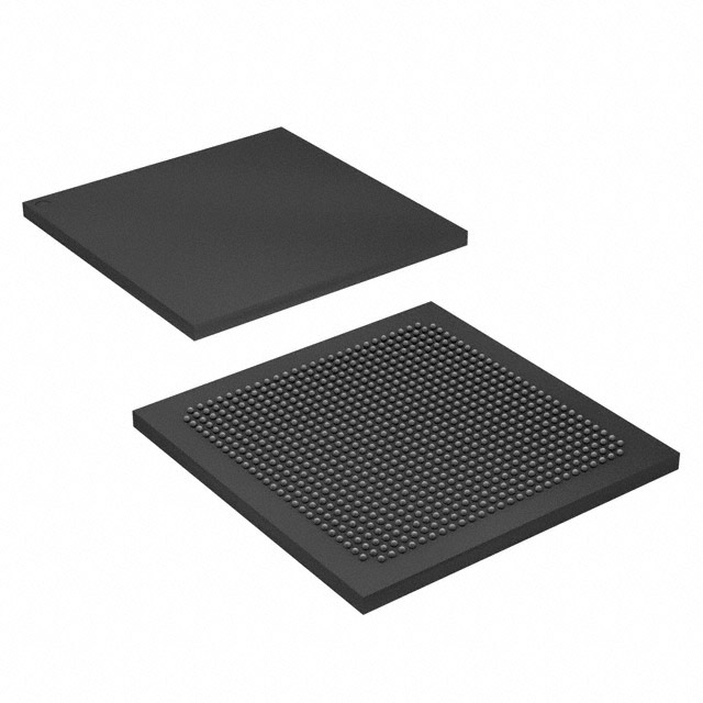
Stratix® IV GX Field Programmable Gate Array (FPGA) IC 564 17661952 291200 1152-BBGA, FCBGA |
|---|---|
| Quantity | 864 Available (as of June 15, 2026) |

| Product Category | Field Programmable Gate Array (FPGA) |
|---|---|
| Manufacturer | Intel |
| Manufacturing Status | Obsolete |
| Manufacturer Standard Lead Time | Contact Us |
| Datasheet |
Specifications & Environmental
| Device Package | 1152-FBGA (35x35) | Grade | Commercial | Operating Temperature | 0°C – 85°C | ||
|---|---|---|---|---|---|---|---|
| Package / Case | 1152-BBGA, FCBGA | Number of I/O | 564 | Voltage | 870 mV - 930 mV | ||
| Mounting Method | Surface Mount | RoHS Compliance | RoHS Compliant | REACH Compliance | REACH Unknown | ||
| Moisture Sensitivity Level | 3 (168 Hours) | Number of LABs/CLBs | 11648 | Number of Logic Elements/Cells | 291200 | ||
| Number of Gates | N/A | ECCN | 3A001A7A | HTS Code | 8542.39.0001 | ||
| Qualification | N/A | Total RAM Bits | 17661952 |
Overview of EP4SGX290HF35C2N – Stratix® IV GX FPGA, 291,200 logic elements (1152-BBGA)
The EP4SGX290HF35C2N is a Stratix IV GX field-programmable gate array (FPGA) in a 1152-BBGA surface-mount package. The device provides a large programmable fabric and on-chip resources suited for designs that require substantial logic capacity, embedded memory, and high I/O density.
Architecture notes in the Stratix IV device handbook highlight integrated high-speed transceivers, DSP blocks, and flexible clocking—making this device appropriate for high-bandwidth, protocol-rich designs that need on-chip processing, buffering, and a wide range of interfaces.
Key Features
- Logic Capacity 291,200 logic elements to implement complex custom logic and large FPGA designs.
- Embedded Memory Approximately 16.8 Mbits of embedded memory (17,661,952 total RAM bits) for on-chip buffering, frame storage, and data staging.
- I/O Density 564 I/O pins to support broad external connectivity and multiple interface endpoints.
- High‑Speed Transceivers & I/O Device handbook documentation describes Stratix IV GX high-speed transceiver features and advanced differential I/O capabilities (including DPA and soft‑CDR) for serial data links and protocol support.
- DSP and Signal Processing On-chip digital signal processing (DSP) block resources are documented for accelerating arithmetic and filtering functions.
- Clocking and PLLs Rich clock networks and integrated PLL resources are provided to support flexible timing architectures and multiple clock domains.
- Package & Mounting 1152-BBGA (FCBGA) surface-mount package; supplier device package specified as 1152-FBGA (35×35).
- Power Core voltage supply range: 0.870 V to 0.930 V.
- Operating Conditions Commercial grade with an operating temperature range of 0 °C to 85 °C.
- Compliance RoHS compliant.
Typical Applications
- High‑Speed Serial Interfaces Implement serial link protocols using the Stratix IV GX transceiver features and differential I/O for data aggregation and protocol bridging.
- On‑Chip Signal Processing Use the device’s DSP resources and large logic capacity for fixed‑point filtering, FFTs, and real‑time processing pipelines.
- External Memory Interfaces Serve as a controller or interface bridge for external memory subsystems, leveraging on‑chip memory and clocking resources for timing-critical buffering.
- Custom Accelerator and Prototyping Develop hardware accelerators or prototype complex logic functions that require large logic arrays and ample embedded RAM.
Unique Advantages
- Substantial Logic Resource: 291,200 logic elements enable implementation of large-scale programmable designs without immediate partitioning across multiple devices.
- Significant On‑Chip Memory: Approximately 16.8 Mbits of embedded RAM reduces reliance on external buffering for many real‑time and packet‑based applications.
- High I/O Count: 564 I/O pins offer broad connectivity for multi‑channel systems, parallel interfaces, and mixed I/O requirements.
- Integrated High‑Speed Interfaces: Stratix IV GX transceiver and differential I/O features support high‑bandwidth serial protocols and advanced signal‑integrity techniques documented in the device handbook.
- Flexible Clocking and DSP Support: On‑chip PLLs, clock networks, and DSP blocks simplify design of multi‑clock and compute‑intensive subsystems.
- Commercial‑Grade, RoHS‑Compliant: Specified for 0 °C to 85 °C operation and RoHS compliance for streamlined regulatory handling in commercial applications.
Why Choose EP4SGX290HF35C2N?
The EP4SGX290HF35C2N combines a large programmable fabric, substantial embedded memory, high I/O density, and documented Stratix IV GX architecture features—making it suitable for designs that demand on‑chip processing, extensive interfacing, and high aggregate data throughput. Its package and power specifications support compact, surface‑mount implementations.
Engineers targeting protocol‑rich, compute‑intensive FPGA designs will find the device handbook’s architecture detail useful for system integration and tuning. The device’s capacity and resources provide a scalable platform for implementing complex logic, DSP acceleration, and multi‑interface controllers within a single FPGA footprint.
Request a quote or submit a pricing and availability inquiry to receive current lead time and purchasing information for EP4SGX290HF35C2N.


Date Founded: 1968
Headquarters: Santa Clara, California, USA
Employees: 130,000+
Revenue: $54.23 Billion
Certifications and Memberships: ISO9001:2015, ISO14001:2015, ISO17025:2017, ISO27001:2022, ISO45001:2018, ISO50001:2018


