
EP4SGX360KF40I3G
| Part Description |
Field Programmable Gate Array (FPGA) IC |
|---|---|
| Quantity | 201 Available (as of June 18, 2026) |

| Product Category | Field Programmable Gate Array (FPGA) |
|---|---|
| Manufacturer | Intel |
| Manufacturing Status | Active |
| Manufacturer Standard Lead Time | 26 Weeks |
| Datasheet |
Specifications & Environmental
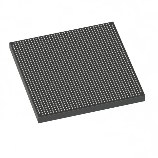
| Device Package | 1517-FBGA (40x40) | Grade | Industrial | Operating Temperature | -40°C – 100°C | ||
|---|---|---|---|---|---|---|---|
| Package / Case | 1517-BBGA, FCBGA | Number of I/O | 744 | Voltage | 870 mV - 930 mV | ||
| Mounting Method | Surface Mount | RoHS Compliance | RoHS Compliant | REACH Compliance | REACH Unaffected | ||
| Moisture Sensitivity Level | 3 (168 Hours) | Number of LABs/CLBs | 14144 | Number of Logic Elements/Cells | 353600 | ||
| Number of Gates | N/A | ECCN | N/A | HTS Code | N/A | ||
| Qualification | N/A | Total RAM Bits | 23105536 |
Overview of EP4SGX360KF40I3G – Field Programmable Gate Array (FPGA) IC
The EP4SGX360KF40I3G is a Stratix IV family FPGA offering a high-density programmable fabric with 353,600 logic elements and approximately 23.1 Mbits of embedded memory. Designed for industrial-grade applications, the device provides extensive I/O capability (744 I/O pins), a compact 1517‑FBGA (40×40) package, and an operating temperature range from −40 °C to 100 °C.
This device is targeted at designs that require significant logic capacity, on-chip memory resources, and robust I/O integration while operating from a low-voltage core supply (870 mV to 930 mV). It leverages the Stratix IV architecture and associated family features such as advanced clocking, DSP blocks, and high-speed transceiver functionality described in the Stratix IV device handbook.
Key Features
- High-density logic — 353,600 logic elements to implement complex custom logic, state machines, and data-paths on a single device.
- Embedded memory — Approximately 23.1 Mbits of on-chip RAM to support buffers, frame storage, and low-latency data handling without immediate external memory dependency.
- Extensive I/O — 744 I/O pins to support wide parallel interfaces, multiple high-speed links, and diverse peripheral connectivity.
- Stratix IV family architecture — Built on the Stratix IV device family platform, including on-chip clock networks, PLLs, DSP blocks, and high-speed transceiver features as described in the device handbook.
- Package & mounting — 1517‑FBGA (40×40) FCBGA package in a surface-mount form factor for compact board designs.
- Industrial temperature grade — Rated for −40 °C to 100 °C operation to meet demanding environmental conditions.
- Low-voltage core supply — Core operating range of 870 mV to 930 mV to match system power-rail planning.
- Regulatory compliance — RoHS compliant for regulatory and manufacturing alignment.
Typical Applications
- High-bandwidth networking — Use the large logic capacity and Stratix IV transceiver and I/O capabilities to implement packet processing, switching logic, and protocol bridging.
- Signal processing and DSP — Leverage abundant logic and on-chip memory alongside family DSP resources for real-time filtering, encoding/decoding, and data aggregation.
- External memory interfaces — Act as an interface controller or aggregator for external memory and peripherals, taking advantage of Stratix IV external memory interface features.
- Industrial automation and control — Deploy in control systems that require sustained operation across a wide temperature range and high I/O counts for sensors, actuators, and fieldbus interfaces.
Unique Advantages
- Large programmable fabric: 353,600 logic elements enable consolidation of multiple functions onto a single FPGA, reducing board complexity and BOM.
- Substantial on-chip memory: Approximately 23.1 Mbits of embedded RAM supports buffering and state storage, minimizing early reliance on external memory devices.
- Broad I/O density: 744 I/O pins allow flexible interface mapping and parallel data paths, easing system partitioning and interface routing.
- Industrial-grade operation: −40 °C to 100 °C rating and RoHS compliance support deployment in demanding environments and regulated manufacturing flows.
- Family-level capabilities: Based on the Stratix IV device family, the device benefits from documented features such as advanced clocking, DSP blocks, and high-speed transceiver technologies for complex system integration.
- Compact, board-ready package: 1517‑FBGA (40×40) surface-mount package helps achieve a compact system footprint while maintaining high pin count.
Why Choose EP4SGX360KF40I3G?
The EP4SGX360KF40I3G positions itself as a high-capacity, industrial-grade FPGA option within the Stratix IV family, combining hundreds of thousands of logic elements, multi-megabit embedded memory, and a large I/O complement in a single FCBGA package. Its documented family features—clock networks, PLLs, DSP blocks, and transceiver support—make it suitable for advanced signal processing, high-throughput interfacing, and complex system control tasks.
This device is well suited for engineering teams designing high-performance, reliable systems that require on-chip integration of logic and memory, broad connectivity, and operation across extended temperature ranges. The use of a Stratix IV family device provides access to family-level documentation and resources to support development and system integration.
Request a quote or submit an inquiry for EP4SGX360KF40I3G to obtain pricing and availability information or to discuss how this device can fit into your next high-density, industrial FPGA design.


Date Founded: 1968
Headquarters: Santa Clara, California, USA
Employees: 130,000+
Revenue: $54.23 Billion
Certifications and Memberships: ISO9001:2015, ISO14001:2015, ISO17025:2017, ISO27001:2022, ISO45001:2018, ISO50001:2018


