
EP4SGX530KH40C3G
| Part Description |
Field Programmable Gate Array (FPGA) IC |
|---|---|
| Quantity | 594 Available (as of October 8, 2026) |

| Product Category | Field Programmable Gate Array (FPGA) |
|---|---|
| Manufacturer | Intel |
| Manufacturing Status | Active |
| Manufacturer Standard Lead Time | 26 Weeks |
| Datasheet |
Specifications & Environmental
| Device Package | 1517-HBGA (42.5x42.5) | Grade | Commercial | Operating Temperature | 0°C – 85°C | ||
|---|---|---|---|---|---|---|---|
| Package / Case | 1517-BBGA, FCBGA | Number of I/O | 744 | Voltage | 870 mV - 930 mV | ||
| Mounting Method | Surface Mount | RoHS Compliance | RoHS Compliant | REACH Compliance | REACH Unaffected | ||
| Moisture Sensitivity Level | 3 (168 Hours) | Number of LABs/CLBs | 21248 | Number of Logic Elements/Cells | 531200 | ||
| Number of Gates | N/A | ECCN | N/A | HTS Code | N/A | ||
| Qualification | N/A | Total RAM Bits | 28033024 |
Overview of EP4SGX530KH40C3G – Field Programmable Gate Array (FPGA) IC
The EP4SGX530KH40C3G is an Intel (Altera) Stratix IV device-class FPGA, optimized for high-bandwidth system integration and on-chip signal processing. It combines a large logic fabric, substantial embedded memory, and extensive I/O capability to support designs that require high aggregate data throughput, protocol flexibility, and integrated DSP resources.
Key Features
- Core Logic — 531,200 logic elements providing a large programmable fabric for complex logic, control and processing implementations.
- Embedded Memory — Approximately 28 Mbits of on-chip RAM for buffering, lookup tables and local data storage.
- I/O Density — 744 user I/O pins to support dense external connectivity and wide parallel interfaces.
- High-Speed Architecture — Device family documentation highlights high-speed transceiver capabilities and support for a wide range of protocols and high aggregate data bandwidth.
- DSP and System Features — Family-level features include digital signal processing blocks, PLLs and comprehensive clock networks for timing and synchronization.
- Power — Specified core voltage supply range of 870 mV to 930 mV to match system power provisioning requirements.
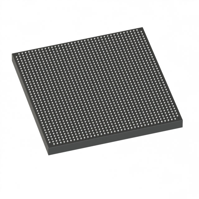
- Package and Mounting — Surface-mount FCBGA package in a 1517-ball HBGA footprint (42.5 × 42.5 mm) for high-pin-count board integration.
- Commercial Grade & Compliance — Commercial temperature grade (0 °C to 85 °C) and RoHS compliant.
Typical Applications
- High‑Bandwidth Communications — Use the device’s high-speed transceiver features and wide I/O to implement protocol bridging, packet processing, and link aggregation.
- Signal Processing & Acceleration — Implement DSP functions and hardware accelerators leveraging the large logic element count and embedded memory.
- External Memory Controllers — Drive complex memory interfaces and buffering with abundant I/O and on-chip RAM.
- System Integration & Prototyping — Combine dense logic, clocking resources and extensive I/O to validate and integrate multi-domain system designs.
Unique Advantages
- High Logic Capacity: 531,200 logic elements enable integration of large, consolidated designs that reduce board-level component count.
- Substantial On-Chip Memory: Approximately 28 Mbits of embedded RAM support local buffering and reduce dependence on external memory for many workloads.
- Extensive I/O Count: 744 I/O pins provide flexibility for parallel interfaces, multiple peripherals, and high-density board routing.
- Designed for High-Speed Systems: Family-level support for high-speed transceivers, protocol support and high aggregate bandwidth helps meet demanding throughput requirements.
- Commercial Temperature & RoHS Compliance: Rated 0 °C to 85 °C and RoHS compliant for standard commercial applications and environmental compliance.
- Robust Packaging: 1517-ball FCBGA/HBGA (42.5 × 42.5 mm) package supports high-pin-count, surface-mount designs for compact boards.
Why Choose EP4SGX530KH40C3G?
The EP4SGX530KH40C3G positions itself as a high-capacity Stratix IV FPGA option for designs that require substantial programmable logic, embedded memory and high I/O density. It is well suited to teams building high-throughput communications, signal processing, and complex system integration solutions that benefit from on-chip DSP resources and flexible clocking.
With a clearly defined core voltage range, commercial temperature rating, and RoHS compliance, this device delivers predictable electrical and environmental characteristics for commercial product lifecycles and development cycles backed by Intel (Altera) device documentation and tool ecosystems.
If you would like pricing, availability or to request a quote for EP4SGX530KH40C3G, submit your inquiry and our team will respond with the next steps to move your project forward.

























Date Founded: 1968
Headquarters: Santa Clara, California, USA
Employees: 130,000+
Revenue: $54.23 Billion
Certifications and Memberships: ISO9001:2015, ISO14001:2015, ISO17025:2017, ISO27001:2022, ISO45001:2018, ISO50001:2018


