
EP4SGX530KH40C4
| Part Description |
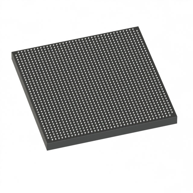
Stratix® IV GX Field Programmable Gate Array (FPGA) IC 744 28033024 531200 1517-BBGA, FCBGA |
|---|---|
| Quantity | 811 Available (as of June 15, 2026) |

| Product Category | Field Programmable Gate Array (FPGA) |
|---|---|
| Manufacturer | Intel |
| Manufacturing Status | Obsolete |
| Manufacturer Standard Lead Time | Contact Us |
| Datasheet |
Specifications & Environmental
| Device Package | 1517-HBGA (42.5x42.5) | Grade | Commercial | Operating Temperature | 0°C – 85°C | ||
|---|---|---|---|---|---|---|---|
| Package / Case | 1517-BBGA, FCBGA | Number of I/O | 744 | Voltage | 870 mV - 930 mV | ||
| Mounting Method | Surface Mount | RoHS Compliance | RoHS non-compliant | REACH Compliance | REACH Unknown | ||
| Moisture Sensitivity Level | 3 (168 Hours) | Number of LABs/CLBs | 21248 | Number of Logic Elements/Cells | 531200 | ||
| Number of Gates | N/A | ECCN | 3A001A7A | HTS Code | 8542.39.0001 | ||
| Qualification | N/A | Total RAM Bits | 28033024 |
Overview of EP4SGX530KH40C4 – Stratix IV GX FPGA, 1517-BBGA FCBGA
The EP4SGX530KH40C4 is a Stratix IV GX field-programmable gate array (FPGA) IC manufactured by Intel. It delivers a high-density, programmable fabric with dedicated I/O and memory resources suitable for designs that require large logic capacity and extensive I/O integration.
Designed for applications that leverage high-speed serial interfaces, embedded memory and DSP functions, this commercial-grade device emphasizes integration and performance within a 1517-BBGA (FCBGA) package.
Key Features
- Logic Capacity — 531,200 logic elements to implement large, complex designs and system-on-chip style integrations.
- Embedded Memory — Approximately 28 Mbits of embedded memory available on-chip for buffering, packet storage, and local data structures.
- I/O Density — 744 user I/O pins to support broad peripheral connectivity and multi-channel interfaces.
- High-speed Family Features — Part of the Stratix IV GX device family with architecture-level support for high-speed transceivers and protocol-oriented I/O (as documented in the device handbook).
- DSP and Clocking — Architecture includes dedicated DSP resources and programmable clocking elements for signal processing and timing management (see device handbook excerpts for family-level details).
- Power and Supply — Core voltage supply specified between 870 mV and 930 mV for the device core power domain.
- Package and Mounting — 1517-BBGA FCBGA package; supplier device package listed as 1517-HBGA with 42.5 × 42.5 mm footprint; surface-mount mounting type.
- Operating Range and Grade — Commercial grade device with an operating temperature range of 0 °C to 85 °C and RoHS compliance.
Typical Applications
- High-speed Serial Communications — Implement multi-protocol serial links and transceiver-based interfaces using the Stratix IV GX family features for aggregate bandwidth.
- External Memory Interface Controllers — Serve as a programmable controller for external memory subsystems leveraging abundant logic and on-chip RAM.
- Digital Signal Processing — Deploy DSP pipelines and custom signal-processing blocks using the device family’s DSP resources and large logic fabric.
- System Integration — Integrate complex glue logic, protocol bridging, and I/O consolidation in a single FPGA to reduce board-level component count.
Unique Advantages
- High logic density: 531,200 logic elements enable consolidation of multiple functions into one device, reducing system complexity.
- Significant on-chip memory: Approximately 28 Mbits of embedded RAM supports local buffering and state storage without immediate dependence on external memory.
- Extensive I/O: 744 I/O pins accommodate broad peripheral and multi-channel interface requirements for complex systems.
- Family-level high-speed features: As a Stratix IV GX device, it benefits from architecture features documented for high aggregate data bandwidth and protocol support.
- Compact FCBGA package: 1517-BBGA footprint with supplier package dimensions (42.5 × 42.5 mm) offers a high-density board-level solution for surface-mount assembly.
- Commercial readiness and compliance: Commercial temperature grade (0 °C to 85 °C) and RoHS compliance simplify integration into mainstream electronic products.
Why Choose EP4SGX530KH40C4?
The EP4SGX530KH40C4 positions itself as a high-density Stratix IV GX FPGA option for designs that require substantial logic, embedded memory and high I/O counts within a single FCBGA package. Its family-level features for high-speed transceivers, DSP support and programmable clocking make it suitable for systems that demand flexible, high-throughput programmable logic.
This device is well suited to engineering teams building complex communications, signal-processing or system-integration applications that benefit from a scalable FPGA fabric backed by Intel’s Stratix IV GX device documentation and ecosystem.
Request a quote or submit a procurement inquiry to receive pricing and availability details for the EP4SGX530KH40C4.


Date Founded: 1968
Headquarters: Santa Clara, California, USA
Employees: 130,000+
Revenue: $54.23 Billion
Certifications and Memberships: ISO9001:2015, ISO14001:2015, ISO17025:2017, ISO27001:2022, ISO45001:2018, ISO50001:2018


