
EP4SGX530KH40C4N
| Part Description |
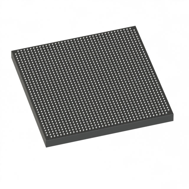
Stratix® IV GX Field Programmable Gate Array (FPGA) IC 744 28033024 531200 1517-BBGA, FCBGA |
|---|---|
| Quantity | 1,000 Available (as of June 15, 2026) |

| Product Category | Field Programmable Gate Array (FPGA) |
|---|---|
| Manufacturer | Intel |
| Manufacturing Status | Obsolete |
| Manufacturer Standard Lead Time | Contact Us |
| Datasheet |
Specifications & Environmental
| Device Package | 1517-HBGA (42.5x42.5) | Grade | Commercial | Operating Temperature | 0°C – 85°C | ||
|---|---|---|---|---|---|---|---|
| Package / Case | 1517-BBGA, FCBGA | Number of I/O | 744 | Voltage | 870 mV - 930 mV | ||
| Mounting Method | Surface Mount | RoHS Compliance | RoHS Compliant | REACH Compliance | REACH Unknown | ||
| Moisture Sensitivity Level | 3 (168 Hours) | Number of LABs/CLBs | 21248 | Number of Logic Elements/Cells | 531200 | ||
| Number of Gates | N/A | ECCN | 3A001A7A | HTS Code | 8542.39.0001 | ||
| Qualification | N/A | Total RAM Bits | 28033024 |
Overview of EP4SGX530KH40C4N – Stratix® IV GX Field Programmable Gate Array (FPGA) IC
The EP4SGX530KH40C4N is a Stratix® IV GX FPGA from Intel, delivered in a 1517-ball BGA (FCBGA) package. It provides a high-density programmable logic fabric combined with on-chip memory and extensive I/O for demanding digital designs.
With 531,200 logic elements, approximately 28.03 Mbits of embedded memory and 744 user I/O pins, this device is well suited to designs that require large logic capacity, substantial on-chip RAM and broad external connectivity. The device operates from a core supply between 870 mV and 930 mV and is specified for commercial temperatures (0 °C to 85 °C).
Key Features
- Core Capacity — 531,200 logic elements provide large-scale programmable logic resources for complex RTL implementations and system integration.
- Embedded Memory — Approximately 28.03 Mbits of on-chip RAM to support data buffering, packet buffering and lookup tables without relying solely on external memory.
- I/O Density — 744 user I/O pins enabling extensive external interfacing and parallel data buses.
- Transceiver, DSP and Memory Subsystems — Device documentation includes transceiver performance specifications, DSP block specifications and TriMatrix memory block specifications to support high-speed serial links, signal processing and embedded memory architectures.
- Clocking and Timing — Clock tree and PLL specifications are provided in the device handbook for deterministic timing and flexible clock management.
- Package and Mounting — 1517-BBGA (FCBGA) package; supplier device package listed as 1517-HBGA (42.5 × 42.5 mm). Surface-mount package suitable for modern PCB assembly.
- Power and Operating Range — Core supply range from 0.870 V to 0.930 V; commercial-grade operation from 0 °C to 85 °C. RoHS-compliant.
- Configuration and Support — Device documentation includes configuration and JTAG specifications along with device handbook material for system integration and validation.
Typical Applications
- High-density digital systems — Use the device’s large logic capacity and on-chip RAM to integrate complex control, data-path and glue logic into a single FPGA.
- Signal processing and compute acceleration — DSP block specifications and abundant logic elements enable accelerated arithmetic and filtering implementations.
- High-bandwidth interfaces — Extensive I/O and transceiver performance documentation support designs requiring multiple external interfaces and high-speed serial links.
Unique Advantages
- Large programmable fabric: 531,200 logic elements let you consolidate multiple functions into a single device, reducing board-level part count.
- Significant embedded memory: Approximately 28.03 Mbits of on-chip RAM reduces reliance on external memory for buffering and lookup tables, improving system latency and simplifying PCB routing.
- High I/O count: 744 user I/Os enable flexible connectivity to peripherals, memory devices and high-pin-count interfaces without multiplexing compromises.
- Comprehensive device documentation: The Stratix IV device handbook provides DC/switching characteristics, PLL, clock tree, transceiver, DSP and memory block specifications to aid deterministic design and verification.
- Compact BGA package: 1517-ball FCBGA in a 42.5 × 42.5 mm supplier package supports dense system designs with surface-mount assembly.
- Regulatory readiness: RoHS-compliant construction supports environmentally conscious manufacturing requirements.
Why Choose EP4SGX530KH40C4N?
The EP4SGX530KH40C4N combines very large logic capacity, substantial embedded memory and a high I/O count in a single Stratix IV GX FPGA package, making it a strong candidate for designs that require integration of complex logic, signal processing and multiple external interfaces. Its documented subsystems — including transceivers, DSP blocks, TriMatrix memory and PLL/clock-tree specifications — support engineering teams in implementing deterministic, high-performance designs.
This device is positioned for commercial-grade systems where on-chip resources, I/O density and vendor documentation are critical to reducing system complexity and shortening development cycles. The Intel Stratix IV handbook and device datasheet provide the technical details needed for validation and long-term support.
Request a quote or submit a pricing inquiry to obtain availability and lead-time information for EP4SGX530KH40C4N. Our team can provide component pricing and delivery details to support your procurement and design schedules.


Date Founded: 1968
Headquarters: Santa Clara, California, USA
Employees: 130,000+
Revenue: $54.23 Billion
Certifications and Memberships: ISO9001:2015, ISO14001:2015, ISO17025:2017, ISO27001:2022, ISO45001:2018, ISO50001:2018


