
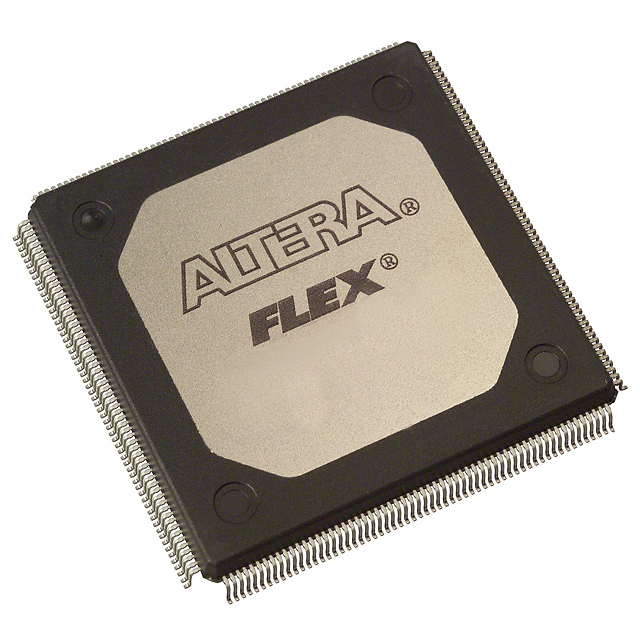
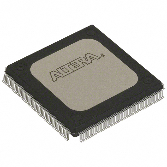
EPF10K20TC144-3N
| Part Description |
FLEX-10K® Field Programmable Gate Array (FPGA) IC 102 12288 1152 144-LQFP |
|---|---|
| Quantity | 409 Available (as of June 15, 2026) |

| Product Category | Field Programmable Gate Array (FPGA) |
|---|---|
| Manufacturer | Intel |
| Manufacturing Status | Obsolete |
| Manufacturer Standard Lead Time | Contact Us |
| Datasheet |
Specifications & Environmental
| Device Package | 144-TQFP (20x20) | Grade | Commercial | Operating Temperature | 0°C – 70°C | ||
|---|---|---|---|---|---|---|---|
| Package / Case | 144-LQFP | Number of I/O | 102 | Voltage | 4.75 V - 5.25 V | ||
| Mounting Method | Surface Mount | RoHS Compliance | Unknown | REACH Compliance | REACH Unaffected | ||
| Moisture Sensitivity Level | 3 (168 Hours) | Number of LABs/CLBs | 144 | Number of Logic Elements/Cells | 1152 | ||
| Number of Gates | 63000 | ECCN | 3A991D | HTS Code | 8542.39.0001 | ||
| Qualification | N/A | Total RAM Bits | 12288 |
Overview of EPF10K20TC144-3N – FLEX-10K® Field Programmable Gate Array (FPGA) IC 102 12288 1152 144-LQFP
The EPF10K20TC144-3N is a FLEX-10K family field programmable gate array (FPGA) from Intel. It combines a dedicated logic array and embedded memory resources to implement configurable logic, on-chip RAM, and system-level functions for embedded designs.
Designed as a 5.0 V device with surface-mount 144-LQFP packaging, this commercial-grade FPGA provides 1,152 logic elements across 144 logic array blocks, 12,288 total RAM bits, and 102 user I/O pins—well suited for system integration, embedded memory functions, and configurable peripheral logic within commercial temperature ranges.
Key Features
- Programmable logic – 1,152 logic elements implemented across 144 logic array blocks (LABs) and approximately 63,000 gates for configurable logic functions.
- Embedded memory – 12,288 total RAM bits of on-chip memory suitable for implementing buffers, small lookup tables, and other megafunctions.
- I/O and interfacing – 102 user I/O pins with individual tri-state control options described by the FLEX 10K family architecture.
- Supply and power – Specified for a 5.0 V supply (4.75 V to 5.25 V), matching 5.0 V system environments.
- System and configuration – Supports in-circuit reconfigurability (ICR) and built-in JTAG boundary-scan circuitry for programming and test without consuming device logic.
- Performance fabric – Family-level features include FastTrack interconnect, dedicated carry and cascade chains, and low-skew clock distribution to support common arithmetic and high-fan-in logic functions.
- Package and mounting – Surface-mount 144-LQFP package (supplier device package: 144-TQFP 20×20) for compact board implementations.
- Operational grade and environment – Commercial grade with an operating temperature range of 0 °C to 70 °C and RoHS compliance.
- Design tooling support – FLEX 10K family is supported by Altera development systems offering automatic place-and-route and megafunction support as described in the family datasheet.
Typical Applications
- Embedded system integration – Use the part where on-chip configurable logic and embedded RAM are required to integrate custom peripherals and glue logic into a single programmable device.
- Memory and buffer functions – Implement small embedded buffers, FIFOs, and lookup tables using the 12,288 bits of on-chip RAM and dedicated array resources.
- Peripheral control and glue logic – Provide flexible I/O handling and protocol adaptation with the device’s programmable logic and 102 user I/Os.
- Prototyping and development – Leverage in-circuit reconfigurability and JTAG boundary-scan to iterate hardware designs and validate logic in-system.
Unique Advantages
- Configurable logic density – 1,152 logic elements and 144 LABs provide a balanced resource set for mid-range programmable logic designs without overprovisioning board space.
- Embedded RAM resources – 12,288 bits of on-chip RAM enable implementation of localized memory functions and megafunctions without external memory.
- System-level configuration and test – Built-in JTAG and support for in-circuit reconfigurability streamline programming and manufacturing test flows.
- Dedicated arithmetic support – Family-level carry and cascade chains accelerate implementation of adders, counters, and comparators in hardware.
- Compact packaging – 144-LQFP surface-mount package (20×20 TQFP footprint) simplifies board layout while providing ample I/O for many embedded applications.
- Toolchain and megafunction support – Supported by Altera development systems for automatic place-and-route and prebuilt megafunctions to reduce development time.
Why Choose EPF10K20TC144-3N?
The EPF10K20TC144-3N positions itself as a mid-density, commercial-grade FPGA suited to designers who need configurable logic, embedded memory, and reliable system-level features in a 5.0 V platform. Its combination of 1,152 logic elements, 12,288 bits of RAM, and 102 I/O pins in a 144-LQFP package makes it appropriate for embedded control, peripheral glue logic, and memory-centric megafunctions.
With in-circuit reconfigurability, JTAG boundary-scan, and supported development tools, this FLEX-10K device enables iterative development and system integration while reducing external component count and simplifying board-level design decisions for commercial embedded products.
To request pricing, check availability, or submit a quote request for EPF10K20TC144-3N, please request a quote or submit a procurement inquiry and a representative will follow up with details.


Date Founded: 1968
Headquarters: Santa Clara, California, USA
Employees: 130,000+
Revenue: $54.23 Billion
Certifications and Memberships: ISO9001:2015, ISO14001:2015, ISO17025:2017, ISO27001:2022, ISO45001:2018, ISO50001:2018


