
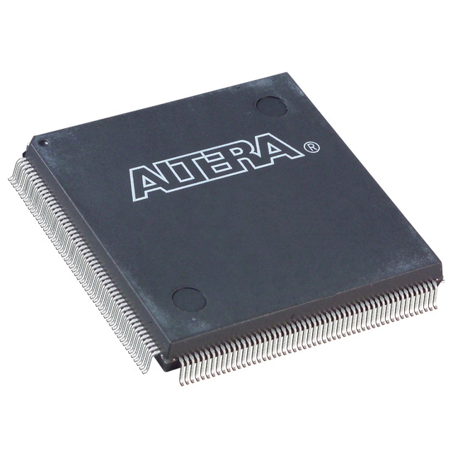
EPF10K30ATC144-1N
| Part Description |
FLEX-10KA® Field Programmable Gate Array (FPGA) IC 102 12288 1728 144-LQFP |
|---|---|
| Quantity | 1,246 Available (as of June 18, 2026) |

| Product Category | Field Programmable Gate Array (FPGA) |
|---|---|
| Manufacturer | Intel |
| Manufacturing Status | Obsolete |
| Manufacturer Standard Lead Time | Contact Us |
| Datasheet |
Specifications & Environmental
| Device Package | 144-TQFP (20x20) | Grade | Commercial | Operating Temperature | 0°C – 70°C | ||
|---|---|---|---|---|---|---|---|
| Package / Case | 144-LQFP | Number of I/O | 102 | Voltage | 3 V - 3.6 V | ||
| Mounting Method | Surface Mount | RoHS Compliance | Unknown | REACH Compliance | REACH Unaffected | ||
| Moisture Sensitivity Level | 3 (168 Hours) | Number of LABs/CLBs | 216 | Number of Logic Elements/Cells | 1728 | ||
| Number of Gates | 69000 | ECCN | 3A991D | HTS Code | 8542.39.0001 | ||
| Qualification | N/A | Total RAM Bits | 12288 |
Overview of EPF10K30ATC144-1N – FLEX-10KA Field Programmable Gate Array (FPGA), 102 I/O, 144-LQFP
The EPF10K30ATC144-1N is a FLEX-10KA family FPGA from Intel, delivered in a 144-pin LQFP package. It combines a logic array and embedded memory resources to enable System-on-a-Programmable-Chip (SOPC) integration and megafunction implementation for embedded designs.
Designed for commercial applications, this device provides reconfigurable logic, on-chip RAM, and a broad set of system features to support embedded logic functions, peripheral interfacing and board-level integration within a 0 °C to 70 °C operating range.
Key Features
- Logic Capacity — 1,728 logic elements and 216 logic array blocks (LABs) provide a balanced array for general-purpose logic implementation.
- Embedded Memory — 12,288 bits of on-chip RAM (EABs available within the FLEX 10K family) for efficient storage of state, buffers and megafunctions.
- Gate Scale — Up to 69,000 maximum system gates to accommodate complex logic and mixed-function designs.
- I/O and Interfaces — 102 user I/O pins with per-pin control options provided by the FLEX 10K family architecture for flexible board-level interfacing.
- Supply and Power — Single-supply operation at 3.0 V to 3.6 V to match common 3.3 V system rails; device is RoHS compliant.
- Package and Mounting — 144-LQFP (supplier device package: 144-TQFP, 20×20 mm) in a surface-mount form factor suitable for compact board layouts.
- System Features — Family-level capabilities include in-circuit reconfigurability (ICR) and IEEE-1149.1 JTAG boundary-scan support for board test and configuration management.
- Commercial Grade — Specified for 0 °C to 70 °C operation and classified as commercial grade for mainstream embedded applications.
Typical Applications
- Embedded Control — Implement control logic, glue functions and custom peripherals using the device’s logic elements and on-chip RAM.
- Interface Bridging — Use the flexible I/O and configurable logic to bridge or adapt between parallel and serial interfaces on mixed-signal boards.
- Prototyping and Development — Leverage in-circuit reconfigurability and JTAG support for rapid firmware iterations and board-level validation.
- SOPC Integration — Integrate megafunctions and memory blocks to consolidate multiple functions into a single programmable chip for reduced BOM and simplified layouts.
Unique Advantages
- Balanced Logic and Memory — 1,728 logic elements paired with 12,288 bits of embedded RAM enable compact implementations of control and buffering functions without external memory.
- Scalable Gate Budget — Up to 69,000 system gates supports designs that need headroom for additional logic or future feature expansion.
- Flexible I/O Count — 102 user I/O pins give designers room to connect multiple peripherals and interfaces directly to the FPGA.
- Board-Level Testability — JTAG boundary-scan support simplifies manufacturing test and in-system programming workflows.
- Surface-Mount Packaging — 144-LQFP / 144-TQFP (20×20) package provides a compact footprint for space-constrained PCBs while remaining accessible for hand and automated assembly.
- Commercial Availability — Commercial-grade temperature range and RoHS compliance make the device suitable for mainstream electronic products and assemblies.
Why Choose EPF10K30ATC144-1N?
The EPF10K30ATC144-1N positions itself as a flexible, reconfigurable building block for embedded and board-level designs that require a balance of logic density and embedded RAM in a compact surface-mount package. Its combination of 1,728 logic elements, approximately 12 Kbits of on-chip memory, and 102 I/O pins provides practical integration for SOPC-style implementations and peripheral interfacing within commercial temperature ranges.
Choose this FPGA when you need proven family-level system features—such as in-circuit reconfigurability and JTAG boundary-scan—combined with a 3.0 V to 3.6 V supply profile and a compact 144-LQFP footprint for production-friendly assemblies.
Request a quote or submit a purchasing inquiry to obtain pricing and availability for EPF10K30ATC144-1N.


Date Founded: 1968
Headquarters: Santa Clara, California, USA
Employees: 130,000+
Revenue: $54.23 Billion
Certifications and Memberships: ISO9001:2015, ISO14001:2015, ISO17025:2017, ISO27001:2022, ISO45001:2018, ISO50001:2018


