
EPF10K30ATC144-2N
| Part Description |
FLEX-10KA® Field Programmable Gate Array (FPGA) IC 102 12288 1728 144-LQFP |
|---|---|
| Quantity | 703 Available (as of June 15, 2026) |

| Product Category | Field Programmable Gate Array (FPGA) |
|---|---|
| Manufacturer | Intel |
| Manufacturing Status | Obsolete |
| Manufacturer Standard Lead Time | Contact Us |
| Datasheet |
Specifications & Environmental
| Device Package | 144-TQFP (20x20) | Grade | Commercial | Operating Temperature | 0°C – 70°C | ||
|---|---|---|---|---|---|---|---|
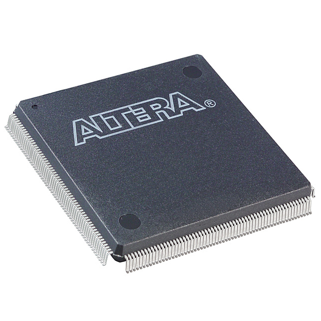
| Package / Case | 144-LQFP | Number of I/O | 102 | Voltage | 3 V - 3.6 V | ||
| Mounting Method | Surface Mount | RoHS Compliance | Unknown | REACH Compliance | REACH Unaffected | ||
| Moisture Sensitivity Level | 3 (168 Hours) | Number of LABs/CLBs | 216 | Number of Logic Elements/Cells | 1728 | ||
| Number of Gates | 69000 | ECCN | 3A991D | HTS Code | 8542.39.0001 | ||
| Qualification | N/A | Total RAM Bits | 12288 |
Overview of EPF10K30ATC144-2N – FLEX-10KA FPGA, 102 I/O, 144-LQFP
The EPF10K30ATC144-2N is a FLEX-10KA field programmable gate array (FPGA) IC from Intel designed for commercial embedded applications. Combining a logic array and embedded memory resources, it is suited for System-on-a-Programmable-Chip (SOPC) integration, efficient implementation of memory-based megafunctions, and general-purpose programmable logic.
With 1,728 logic elements, 12,288 bits of on-chip RAM and 102 user I/O pins in a 144-LQFP surface-mount package, this device targets compact, reconfigurable designs that require moderate density logic and embedded memory at standard commercial operating conditions.
Key Features
- Logic Capacity — 1,728 logic elements and approximately 69,000 gates provide the programmable fabric for combinational and sequential logic implementation.
- Embedded Memory — 12,288 total RAM bits available for on-chip storage and megafunction implementations.
- I/O and Interfaces — 102 user I/O pins with per-pin programmability for output enable and open-drain options; supports MultiVolt I/O interface modes per family documentation.
- Reconfiguration and Test — In-circuit reconfigurability via external configuration device or JTAG port; built-in IEEE 1149.1 JTAG boundary-scan test circuitry for board-level test without consuming device logic.
- System Features — Dedicated carry and cascade chains for arithmetic and high fan-in functions; up to six global clocks and four global clears for synchronous designs.
- Power and Supply — Operates from a 3.0 V to 3.6 V supply range suitable for 3.3-V systems.
- Package and Mounting — 144-LQFP (surface mount) package, supplier package referenced as 144-TQFP (20×20), enabling board-level placement in compact layouts.
- Operating Conditions & Compliance — Commercial grade operation from 0 °C to 70 °C; RoHS compliant.
Typical Applications
- Embedded Systems — SOPC integration and on-chip memory make this device suitable for embedded controllers and custom logic blocks in commercial electronic products.
- Memory-Intensive Functions — Use embedded RAM and EAB-style memory resources for buffering, lookup tables, and specialized memory-based megafunctions.
- Interface Bridging & Peripheral Logic — Programmable I/O and dedicated logic resources support protocol bridging, glue logic, and peripheral control in communications and computing equipment.
- Prototyping and Development — Moderate density logic and standard 144-LQFP packaging facilitate prototyping, evaluation, and integration into development boards.
Unique Advantages
- Balanced Logic and Memory — Combined 1,728 logic elements with 12,288 bits of RAM simplifies implementation of mixed logic and memory functions without external RAM in many designs.
- Reconfigurability — In-circuit reconfigurability and JTAG access allow design updates and debug without board modifications.
- Dedicated Arithmetic and Routing Resources — Carry and cascade chains accelerate adders, counters, and high fan-in logic, reducing design complexity and timing effort.
- Flexible I/O Control — Per-pin tri-state, open-drain options and programmable output slew control support a range of interface requirements on 102 user I/Os.
- Commercial-Friendly Packaging — 144-LQFP surface-mount footprint provides a practical balance of pin count and board space for commercial products.
- Standards-Based Testability — Built-in IEEE 1149.1 JTAG boundary-scan enables board-level test and diagnostics without consuming user logic.
Why Choose EPF10K30ATC144-2N?
The EPF10K30ATC144-2N positions itself as a versatile, commercial-grade FPGA option for designers who need a balance of logic, embedded memory, and flexible I/O in a compact package. Its combination of 1,728 logic elements, 12,288 bits of RAM, and 102 user I/Os supports a wide range of embedded and interface-focused applications while providing reconfigurability and built-in testability.
Engineers building commercial embedded products will find this Intel FLEX-10KA device suitable for designs that require on-chip memory megafunctions, programmable logic integration, and standard 3.3-V system compatibility with RoHS compliance.
Request a quote or submit a product inquiry to learn about availability, pricing, and lead times for the EPF10K30ATC144-2N.


Date Founded: 1968
Headquarters: Santa Clara, California, USA
Employees: 130,000+
Revenue: $54.23 Billion
Certifications and Memberships: ISO9001:2015, ISO14001:2015, ISO17025:2017, ISO27001:2022, ISO45001:2018, ISO50001:2018


