
EPF10K30ATC144-3N
| Part Description |
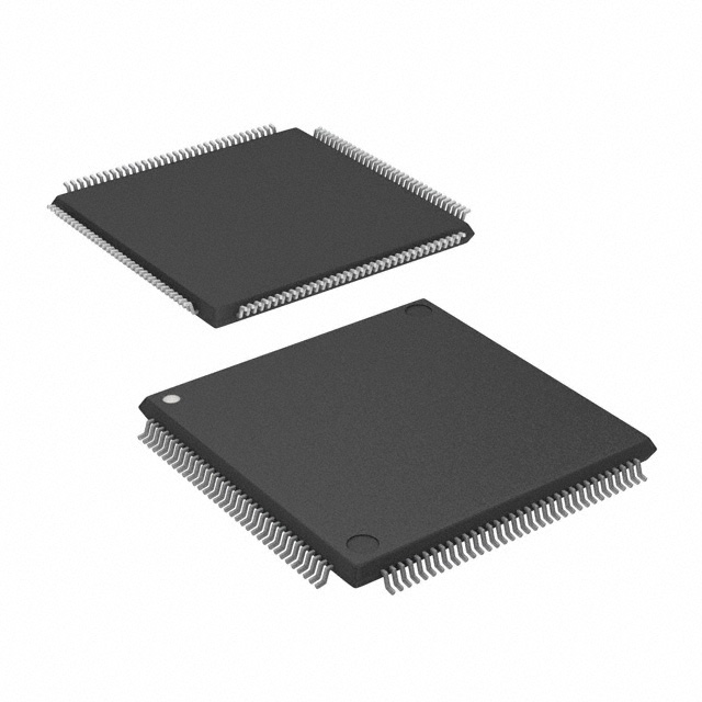
FLEX-10KA® Field Programmable Gate Array (FPGA) IC 102 12288 1728 144-LQFP |
|---|---|
| Quantity | 271 Available (as of October 7, 2026) |

| Product Category | Field Programmable Gate Array (FPGA) |
|---|---|
| Manufacturer | Intel |
| Manufacturing Status | Obsolete |
| Manufacturer Standard Lead Time | Contact Us |
| Datasheet |
Specifications & Environmental
| Device Package | 144-TQFP (20x20) | Grade | Commercial | Operating Temperature | 0°C – 70°C | ||
|---|---|---|---|---|---|---|---|
| Package / Case | 144-LQFP | Number of I/O | 102 | Voltage | 3 V - 3.6 V | ||
| Mounting Method | Surface Mount | RoHS Compliance | Unknown | REACH Compliance | REACH Unaffected | ||
| Moisture Sensitivity Level | 3 (168 Hours) | Number of LABs/CLBs | 216 | Number of Logic Elements/Cells | 1728 | ||
| Number of Gates | 69000 | ECCN | 3A991D | HTS Code | 8542.39.0001 | ||
| Qualification | N/A | Total RAM Bits | 12288 |
Overview of EPF10K30ATC144-3N – FLEX-10KA Field Programmable Gate Array (FPGA) IC, 102 I/Os, 12,288-bit RAM, 1,728 Logic Elements, 144‑LQFP
The EPF10K30ATC144-3N is a FLEX-10KA family FPGA manufactured by Intel. It combines a logic array and embedded memory array to support custom digital logic, on-chip storage, and system-level integration for commercial applications.
With 1,728 logic elements, 12,288 total RAM bits, and 102 I/O pins in a 144‑LQFP surface-mount package, this device targets designs that require moderate logic density, flexible I/O, and in-circuit reconfigurability.
Key Features
- Logic Capacity — 1,728 logic elements and 216 LABs provide the programmable logic resources needed for glue logic, control functions, and mid-scale custom logic implementations.
- On‑chip Memory — 12,288 total RAM bits of embedded memory support buffering, small FIFOs, and state storage without external RAM.
- Gate Density — Specified with 69,000 gates, enabling mapping of larger logic functions when required by tool flows and system partitioning.
- I/O and Voltage — 102 user I/O pins with a 3.0 V to 3.6 V supply range for 3.3 V designs; series documentation describes flexible I/O features such as individual tri‑state control, open‑drain options, and programmable slew-rate control.
- System Integration — Series-level features include an embedded array for megafunctions and support for in-circuit reconfigurability via external configuration device, intelligent controller, or JTAG port.
- Built‑in Test and Clocking — Family datasheet describes built-in JTAG boundary-scan (IEEE Std. 1149.1) circuitry and low-skew clock distribution options for predictable timing.
- Package & Mounting — 144‑LQFP (surface mount) package, supplier package listed as 144‑TQFP (20×20), suitable for compact board layouts.
- Commercial Grade — Rated for 0 °C to 70 °C operating temperature and RoHS compliant for standard commercial applications.
Typical Applications
- Prototyping and Development — Use as a reconfigurable platform for validating custom logic, interfaces, and system prototypes where mid-scale logic and embedded memory are required.
- Peripheral Interface and Glue Logic — Ideal for implementing bus bridging, protocol adaptation, and custom peripheral control using available I/Os and on-chip memory.
- Control and Sequencing — Implement finite-state machines, control sequencers, and timing-critical logic with dedicated clock distribution and logic resources.
- Embedded Function Acceleration — Offload specialized, compute‑intensive functions into programmable logic blocks and use embedded RAM for local data buffering.
Unique Advantages
- Balanced Resource Mix: Combines 1,728 logic elements with 12,288 bits of embedded RAM to support both logic and data storage within the same device.
- Flexible I/O and Voltage Support: 102 user I/Os and a 3.0 V–3.6 V supply range accommodate common 3.3 V system interfaces and signal requirements.
- In‑Circuit Reconfigurability: Support for reconfiguration via external device, controller, or JTAG enables iterative firmware updates and field adjustments without board-level changes.
- Testability and Integration: Built-in JTAG boundary-scan simplifies board-level testing and integration during development and manufacturing.
- Compact Packaging: 144‑LQFP surface-mount package offers a compact footprint for space-constrained commercial products.
Why Choose EPF10K30ATC144-3N?
The EPF10K30ATC144-3N provides a practical balance of logic, embedded memory, and I/O for commercial designs that need mid-range FPGA capability in a compact package. Its combination of 1,728 logic elements, 12,288 bits of on-chip RAM, and 102 user I/Os makes it suitable for prototyping, peripheral logic, control systems, and embedded acceleration tasks.
Designed for commercial temperatures and RoHS compliance, this FLEX‑10KA device offers reconfigurability, built‑in test support, and the package choices needed to integrate programmable logic into production designs while leveraging established family features documented in the series datasheet.
Request a quote or submit an inquiry to check availability, pricing, and lead time for EPF10K30ATC144-3N.
























Date Founded: 1968
Headquarters: Santa Clara, California, USA
Employees: 130,000+
Revenue: $54.23 Billion
Certifications and Memberships: ISO9001:2015, ISO14001:2015, ISO17025:2017, ISO27001:2022, ISO45001:2018, ISO50001:2018


