
EPF6010AFC256-3
| Part Description |
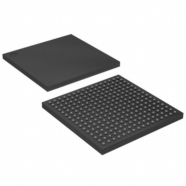
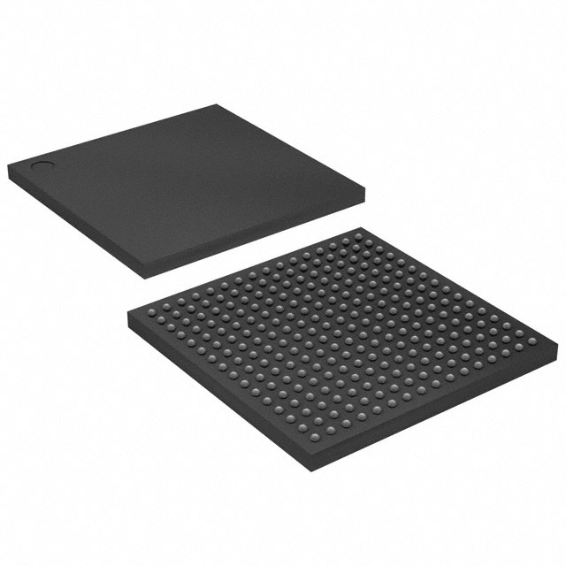
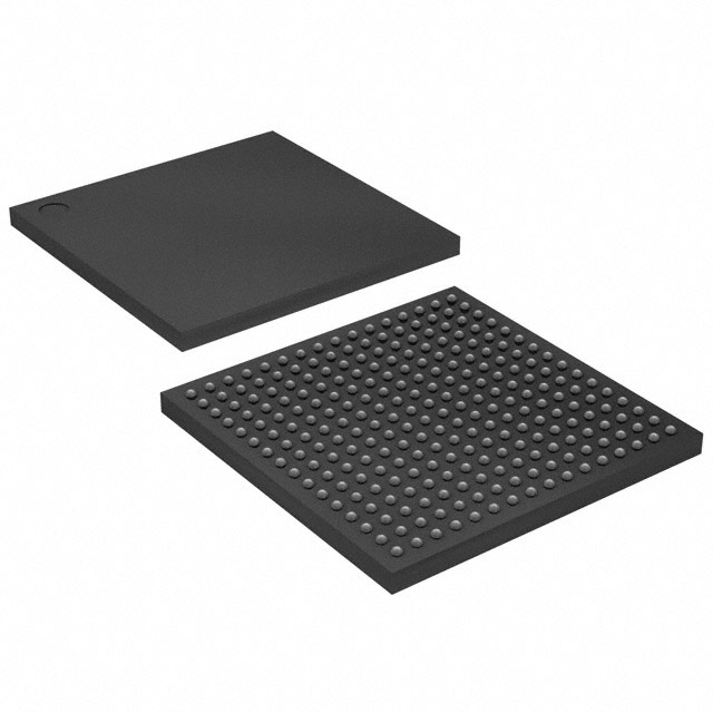
FLEX 6000 Field Programmable Gate Array (FPGA) IC 171 880 256-BGA |
|---|---|
| Quantity | 999 Available (as of October 8, 2026) |
| Product Category | Field Programmable Gate Array (FPGA) |
|---|---|
| Manufacturer | Intel |
| Manufacturing Status | Obsolete |
| Manufacturer Standard Lead Time | Contact Us |
| Datasheet |
Specifications & Environmental
| Device Package | 256-FBGA (17x17) | Grade | Commercial | Operating Temperature | 0°C – 85°C | ||
|---|---|---|---|---|---|---|---|
| Package / Case | 256-BGA | Number of I/O | 171 | Voltage | 3 V - 3.6 V | ||
| Mounting Method | Surface Mount | RoHS Compliance | Unknown | REACH Compliance | REACH Unknown | ||
| Moisture Sensitivity Level | 3 (168 Hours) | Number of LABs/CLBs | 88 | Number of Logic Elements/Cells | 880 | ||
| Number of Gates | 10000 | ECCN | OBSOLETE | HTS Code | 0000.00.0000 | ||
| Qualification | N/A |
Overview of EPF6010AFC256-3 – FLEX 6000 Field Programmable Gate Array (FPGA) IC 171 880 256-BGA
The EPF6010AFC256-3 is a FLEX 6000 series FPGA offering a register-rich, LUT-based architecture (OptiFLEX) for reprogrammable logic in commercial applications. It targets low-cost gate-array replacements, prototyping and design testing where in-circuit reconfigurability and flexible I/O are required.
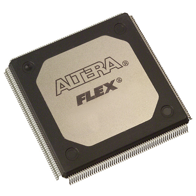
Key on-chip resources include 880 logic elements and approximately 10,000 typical gates, a built-in low-skew clock distribution tree, and support for JTAG boundary-scan. The device ships in a 256-ball BGA (17×17) package and is RoHS compliant.
Key Features
- Core architecture Register-rich, LUT-based OptiFLEX architecture designed to increase device area efficiency and support fast design changes.
- Logic capacity 880 logic elements and approximately 10,000 typical gates suitable for compact programmable logic designs.
- I/O and interfacing 171 I/O pins with individual tri-state output enable control and programmable output slew-rate to manage signal integrity.
- In-system configurability In-circuit reconfigurability (ICR) via external configuration device or intelligent controller for iterative prototyping and field updates.
- Testability and tools Built-in JTAG boundary-scan test (IEEE Std. 1149.1-1990) and 100% functional device testing reduce board-level debug time.
- Clock and arithmetic support Built-in low-skew clock distribution and dedicated carry/cascade chains for efficient implementation of adders, counters and high-fan-in logic.
- Interconnect FastTrack continuous routing structure for predictable interconnect delays and automatic use of dedicated chains by design tools.
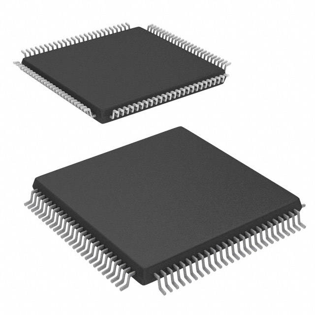
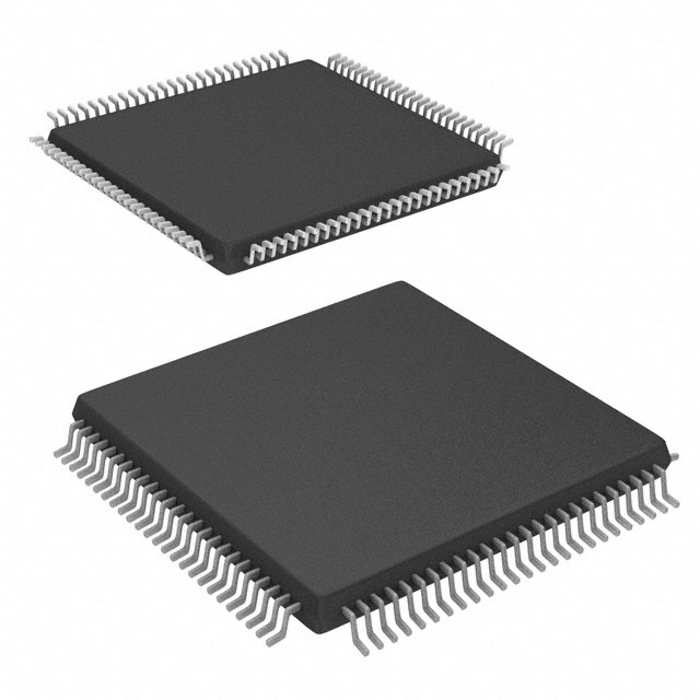
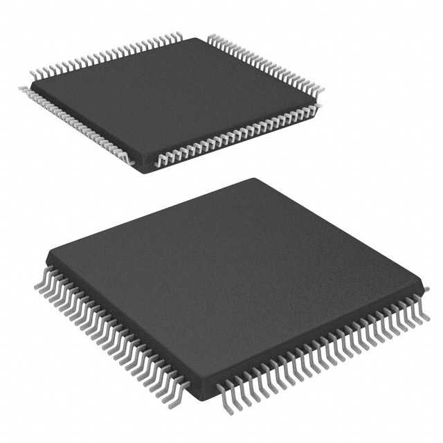
- Package and assembly 256-ball BGA (256-FBGA, 17×17) surface-mount package for compact PCB footprints and high pin density.
- Power & voltage Supply voltage range 3 V to 3.6 V; commercial-grade operation across 0 °C to 85 °C.
- Compliance RoHS compliant.
Typical Applications
- Prototyping & design validation Use the device for rapid iteration and functional testing of logic designs with in-circuit reconfiguration and JTAG support.
- Low-cost gate-array replacement Replace fixed gate-array parts with a reprogrammable solution to enable late-stage changes and reduce NRE risk.
- Interface bridging Implement glue logic and voltage-domain bridging using flexible I/O and programmable output slew control.
- Control and sequencing logic Implement compact control functions, state machines, and arithmetic operations using the device’s logic elements and dedicated chains.
Unique Advantages
- Reconfigurability for fast iteration: In-circuit reconfiguration lets you update functionality without replacing hardware, speeding prototyping and field fixes.
- Compact, efficient architecture: OptiFLEX and LUT-based design delivers area efficiency that supports competitive gate counts in a small package.
- Proven testability: 100% functional testing and integrated JTAG boundary-scan reduce board bring-up time and simplify production test.
- Predictable timing and arithmetic support: Low-skew global paths plus dedicated carry and cascade chains simplify implementation of timing-sensitive logic and arithmetic units.
- High I/O density in a compact package: 171 I/O pins in a 256-ball FBGA (17×17) enable dense signal routing while minimizing PCB area.
- Commercial temperature and RoHS compliance: Rated for 0 °C to 85 °C operation and RoHS compliant for mainstream commercial designs.
Why Choose EPF6010AFC256-3?
The EPF6010AFC256-3 is positioned for design teams seeking a reprogrammable, commercially graded FPGA that balances logic capacity, I/O density, and board-level testability. Its OptiFLEX architecture, dedicated arithmetic chains, and comprehensive JTAG support make it suitable for prototyping, low-cost gate-array replacement, and compact control logic implementations.
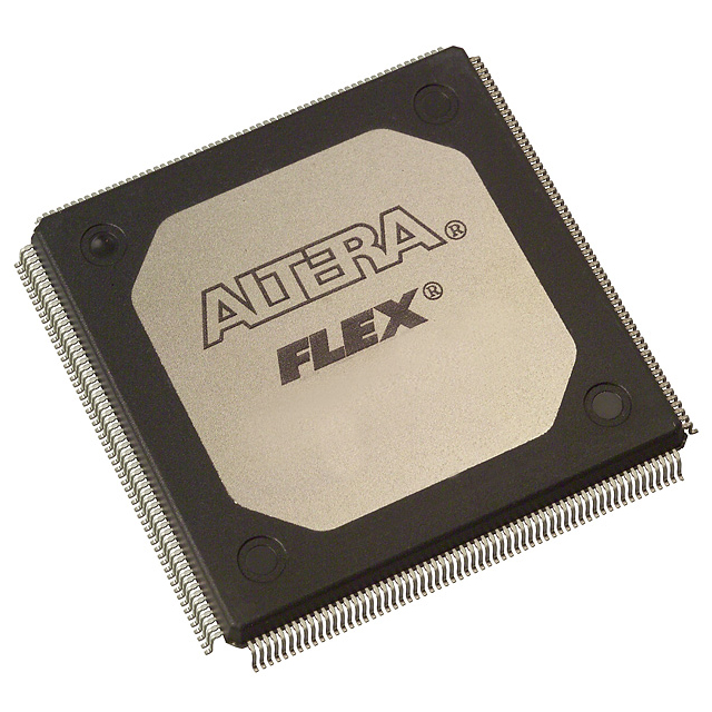
Supported by Altera’s development tool ecosystem and automatic place-and-route flows, the device is aimed at engineers who need fast design iteration, predictable routing, and a compact BGA footprint for space-constrained PCBs.
Request a quote or submit an RFQ for the EPF6010AFC256-3 to get pricing, availability, and lead-time information for your next design.






















Date Founded: 1968
Headquarters: Santa Clara, California, USA
Employees: 130,000+
Revenue: $54.23 Billion
Certifications and Memberships: ISO9001:2015, ISO14001:2015, ISO17025:2017, ISO27001:2022, ISO45001:2018, ISO50001:2018


