
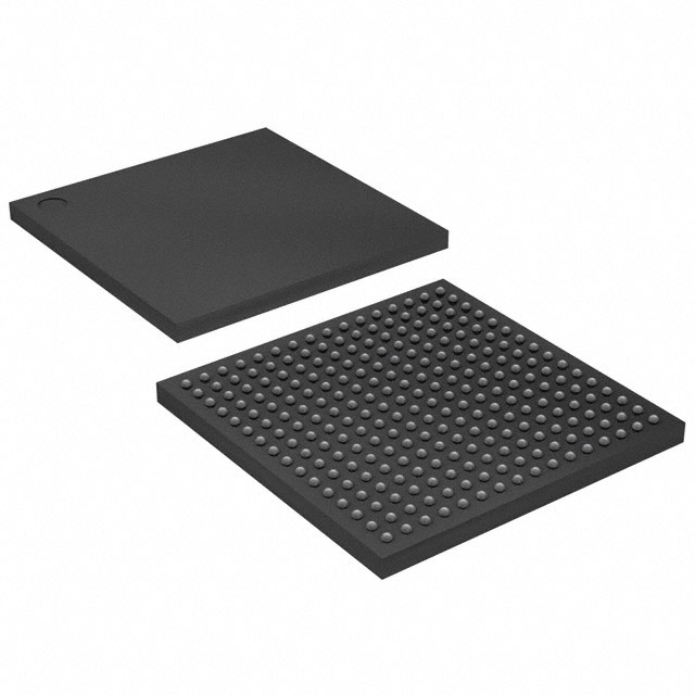
EPF6010AFC256-1
| Part Description |
FLEX 6000 Field Programmable Gate Array (FPGA) IC 171 880 256-BGA |
|---|---|
| Quantity | 1,100 Available (as of June 10, 2026) |
| Product Category | Field Programmable Gate Array (FPGA) |
|---|---|
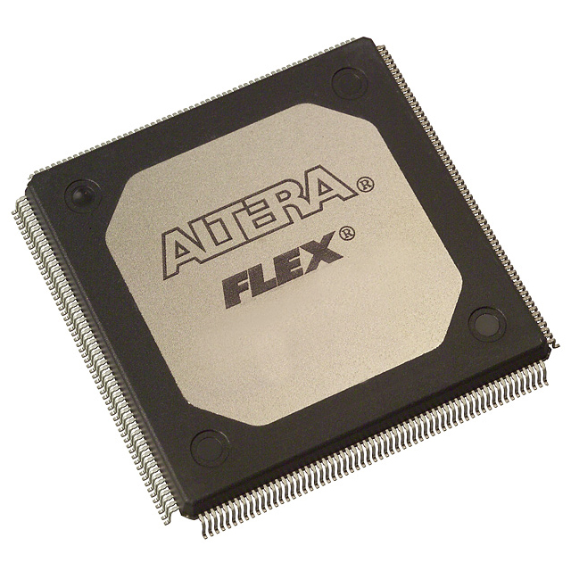
| Manufacturer | Intel |
| Manufacturing Status | Obsolete |
| Manufacturer Standard Lead Time | Contact Us |
| Datasheet |
Specifications & Environmental
| Device Package | 256-FBGA (17x17) | Grade | Commercial | Operating Temperature | 0°C – 85°C | ||
|---|---|---|---|---|---|---|---|
| Package / Case | 256-BGA | Number of I/O | 171 | Voltage | 3 V - 3.6 V | ||
| Mounting Method | Surface Mount | RoHS Compliance | Unknown | REACH Compliance | REACH Unknown | ||
| Moisture Sensitivity Level | 3 (168 Hours) | Number of LABs/CLBs | 88 | Number of Logic Elements/Cells | 880 | ||
| Number of Gates | 10000 | ECCN | OBSOLETE | HTS Code | 0000.00.0000 | ||
| Qualification | N/A |
Overview of EPF6010AFC256-1 – FLEX 6000 FPGA, 880 logic elements, 256-FBGA
The EPF6010AFC256-1 is a FLEX 6000 family field-programmable gate array delivering 880 logic elements (approximately 10,000 typical gates) in a compact 256-ball FBGA (17×17) surface-mount package. The device is built on a register-rich, LUT-based OptiFLEX architecture and targets low-cost gate-array replacement, rapid prototyping, and reconfigurable system functions.
Designed for commercial applications, the device supports 171 I/O pins, a 3.0–3.6 V supply range, and an operating temperature range of 0 °C to 85 °C. It combines flexible configuration and test features with dedicated routing resources for predictable timing and arithmetic performance.
Key Features
- Core architecture Register-rich, look-up table (LUT)-based OptiFLEX architecture that minimizes die area while providing reprogrammable logic.
- Logic capacity Approximately 880 logic elements and about 10,000 typical gates as characterized for the FLEX 6000 family device.
- I/O and signaling 171 general-purpose I/O pins with individual tri-state output enable control and programmable output slew-rate to help manage signal integrity and system interfacing.
- Clock and routing Built-in low-skew clock distribution and four low-skew global paths, plus the FastTrack interconnect structure for predictable routing delays.
- Arithmetic and high-fan-in logic Dedicated carry chain and cascade chain resources for efficient adders, counters, comparators, and high-fan-in logic functions.
- Configuration and test Supports in-circuit reconfigurability via external configuration device or intelligent controller and includes IEEE Std. 1149.1 JTAG boundary-scan test circuitry without consuming additional device logic.
- Supply and power Operates from 3.0 V to 3.6 V. Family documentation notes low-power standby behavior for reduced idle current.
- Package and environmental 256-FBGA (17×17) surface-mount package, commercial grade, RoHS compliant, and specified for 0 °C to 85 °C operation.
- Quality and compatibility Devices are 100% functionally tested prior to shipment and the FLEX 6000 family provides SameFrame pin-compatibility across densities and pin counts.
Typical Applications
- Prototyping and design validation Reprogrammable SRAM-based logic and in-circuit reconfiguration let development teams iterate firmware and hardware quickly during prototyping and testing phases.
- Gate-array replacement Offers a lower-cost, reprogrammable alternative to fixed gate-array designs for medium-complexity logic integration and volume transitions.
- Glue logic and interface bridging High I/O count and programmable I/O controls enable protocol adaptation, bus bridging, and custom interface functions between subsystems.
- Control and timing-critical functions Dedicated carry and cascade chains plus low-skew global clocks support fast arithmetic and timing-sensitive control logic.
Unique Advantages
- Reconfigurable during development SRAM-based device architecture and in-circuit reconfigurability simplify iterative design changes and late-stage updates without PCB rework.
- Predictable routing and timing FastTrack interconnect, dedicated carry/cascade resources, and a low-skew clock tree help reduce timing uncertainty for critical paths.
- High I/O flexibility 171 I/O pins with individual tri-state control and programmable slew-rate improve interoperability with diverse voltage domains and peripheral devices.
- Compact, production-ready package 256-FBGA (17×17) surface-mount package minimizes board area while supporting production assembly processes for commercial electronics.
- Tested and compatible 100% functional testing at shipment and SameFrame pin-compatibility across the FLEX 6000 family reduce qualification effort when scaling designs across densities.
- RoHS compliant Environmentally compliant for systems requiring lead-free component selection.
Why Choose EPF6010AFC256-1?
The EPF6010AFC256-1 brings a practical combination of reprogrammability, predictable routing, and a compact FBGA package for commercial embedded designs that require medium-density logic integration. Its OptiFLEX architecture and dedicated arithmetic/cascade structures deliver efficient use of silicon area while providing the flexibility needed during prototyping and product iterations.
This device is well suited for teams looking to replace fixed gate-array logic with a reprogrammable solution, implement complex interface logic with abundant I/O, or accelerate development cycles via in-circuit reconfiguration and family-level pin compatibility.
Request a quote or submit an RFQ to evaluate the EPF6010AFC256-1 for your next design.


Date Founded: 1968
Headquarters: Santa Clara, California, USA
Employees: 130,000+
Revenue: $54.23 Billion
Certifications and Memberships: ISO9001:2015, ISO14001:2015, ISO17025:2017, ISO27001:2022, ISO45001:2018, ISO50001:2018


