
EPF6016QC240-3N
| Part Description |
FLEX 6000 Field Programmable Gate Array (FPGA) IC 199 1320 240-BFQFP |
|---|---|
| Quantity | 220 Available (as of June 18, 2026) |

| Product Category | Field Programmable Gate Array (FPGA) |
|---|---|
| Manufacturer | Intel |
| Manufacturing Status | Obsolete |
| Manufacturer Standard Lead Time | Contact Us |
| Datasheet |
Specifications & Environmental
| Device Package | 240-PQFP (32x32) | Grade | Commercial | Operating Temperature | 0°C – 85°C | ||
|---|---|---|---|---|---|---|---|
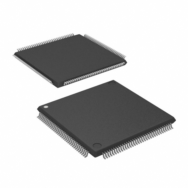
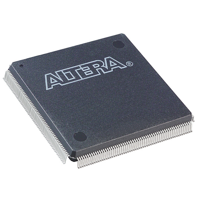
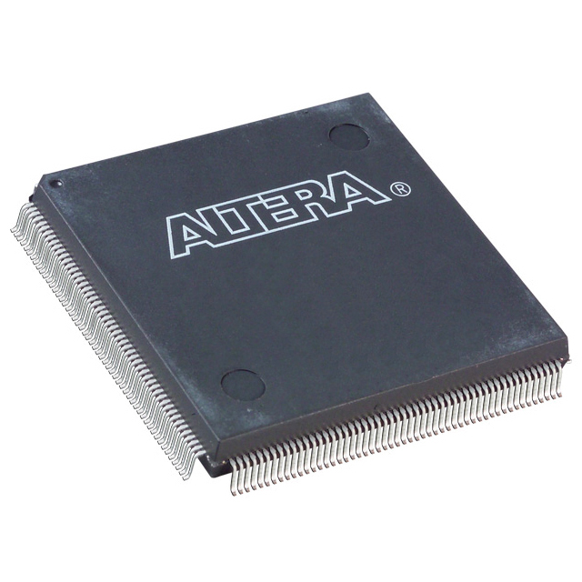
| Package / Case | 240-BFQFP | Number of I/O | 199 | Voltage | 4.75 V - 5.25 V | ||
| Mounting Method | Surface Mount | RoHS Compliance | Unknown | REACH Compliance | REACH Unaffected | ||
| Moisture Sensitivity Level | 3 (168 Hours) | Number of LABs/CLBs | 132 | Number of Logic Elements/Cells | 1320 | ||
| Number of Gates | 16000 | ECCN | 3A991D | HTS Code | 8542.39.0001 | ||
| Qualification | N/A |
Overview of EPF6016QC240-3N – FLEX 6000 Field Programmable Gate Array (FPGA) IC 199 1320 240-BFQFP
The EPF6016QC240-3N is a FLEX 6000 series field programmable gate array designed for low-cost, reprogrammable logic implementations. Based on the OptiFLEX architecture, this 5.0‑V device provides approximately 16,000 typical gates and 1,320 logic elements in a 240‑pin package, supporting in‑circuit reconfiguration and rapid design iteration during prototyping and design testing.
With a high I/O count and built‑in system features such as JTAG boundary‑scan and a low‑skew clock distribution tree, the EPF6016QC240-3N is suited to applications that require flexible, reprogrammable logic and reliable board‑level integration within commercial temperature ranges.
Key Features
- OptiFLEX architecture Efficient LUT‑based architecture that minimizes die size while supporting reconfigurable SRAM elements and fast design changes.
- Logic and density Approximately 16,000 typical gates and 1,320 logic elements for mid‑range logic integration.
- High I/O count 199 programmable I/O pins to support dense peripheral and bus interfacing on a single device.
- Package and mounting 240‑pin BFQFP package (supplier device package listed as 240‑PQFP, 32×32) with surface‑mount mounting for standard PCB assembly.
- Supply and temperature 5.0‑V device with supply range 4.75 V to 5.25 V and commercial operating temperature range of 0 °C to 85 °C.
- System test and debug Industry‑standard JTAG boundary‑scan (IEEE Std. 1149.1) is included without consuming device logic to simplify board test and in‑system debug.
- Programmable I/O controls Individual tri‑state output enable control and programmable output slew‑rate help manage signal integrity and interfacing requirements.
- Deterministic interconnect and arithmetic support FastTrack interconnect, dedicated carry chains and cascade chains enable predictable routing and efficient implementation of adders, counters and high‑fan‑in logic.
- Clocking and low power modes Built‑in low‑skew clock distribution tree and low standby current behavior to support synchronized designs and reduced idle power.
- Quality and compliance 100% functional testing prior to shipment and RoHS compliance.
Typical Applications
- Prototyping and design testing Reprogrammable logic enables rapid iteration and functional changes during board bring‑up and prototype validation.
- Gate array replacement Low‑cost, reprogrammable alternative to high‑volume gate array implementations where fast design changes are needed prior to production.
- In‑system reconfigurable designs In‑circuit reconfigurability supports dynamic updates and functional changes during operation via external configuration devices or controllers.
- Board‑level test and validation Built‑in JTAG boundary‑scan simplifies manufacturing test, diagnostics, and debug without consuming application logic.
Unique Advantages
- Flexible reconfiguration: In‑circuit reconfigurability allows functional updates and design changes without board redesign.
- Rich I/O and package choice: 199 I/O in a 240‑pin surface‑mount package supports dense system interfaces while fitting standard PCB footprints.
- Predictable performance: FastTrack interconnect and dedicated carry/cascade chains provide predictable routing and efficient arithmetic implementation.
- Built‑in test support: IEEE‑compliant JTAG boundary‑scan is available without consuming user logic, simplifying production test and debugging.
- Verified quality: Devices are 100% functionally tested prior to shipment and are RoHS compliant.
- Commercial temperature operation: Designed for commercial applications with an operating range of 0 °C to 85 °C and a stable 5.0‑V supply window.
Why Choose EPF6016QC240-3N?
The EPF6016QC240-3N delivers a balanced combination of logic density, I/O capacity and system features for designers needing a reprogrammable, mid‑density FPGA in a 240‑pin surface‑mount package. Its OptiFLEX architecture, predictable interconnect structures and dedicated arithmetic resources make it appropriate for prototyping, gate array replacement and board‑level designs that require flexible reprogramming and robust test capabilities.
With 1,320 logic elements, approximately 16,000 typical gates, 199 I/O pins, 100% functional testing and RoHS compliance, this device is positioned for commercial embedded and system applications where iterative development, board testability and reliable operation across standard temperature and supply ranges are required.
Request a quote or submit an inquiry to arrange pricing and availability for the EPF6016QC240-3N. Our team can provide lead‑time and ordering information to support your development schedule.


Date Founded: 1968
Headquarters: Santa Clara, California, USA
Employees: 130,000+
Revenue: $54.23 Billion
Certifications and Memberships: ISO9001:2015, ISO14001:2015, ISO17025:2017, ISO27001:2022, ISO45001:2018, ISO50001:2018


