
EPF6016TC144-2N
| Part Description |
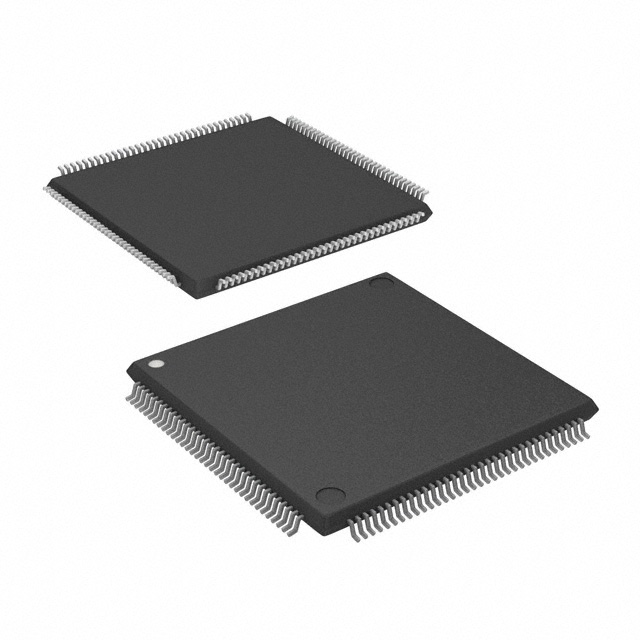
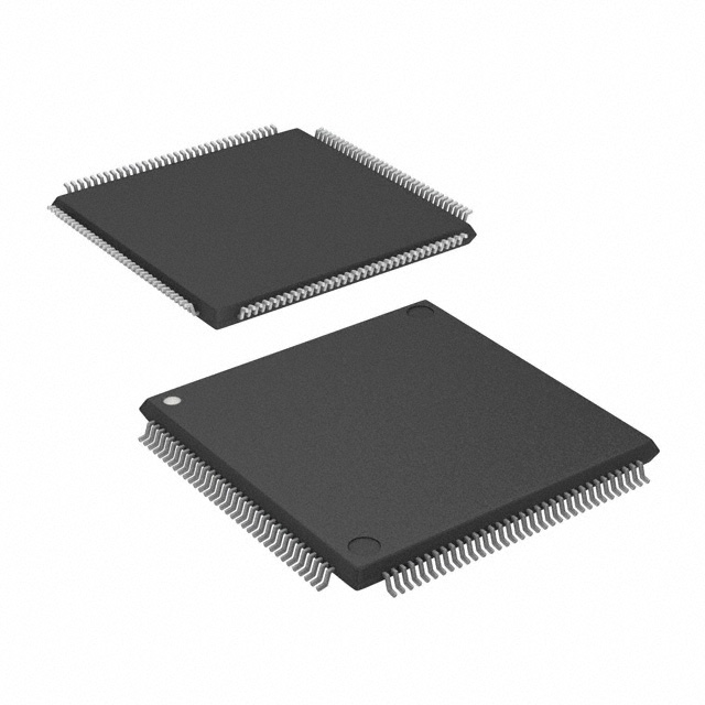
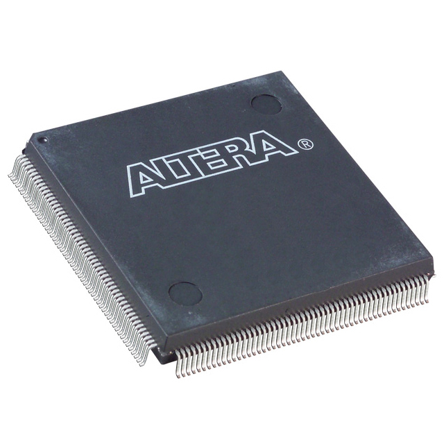
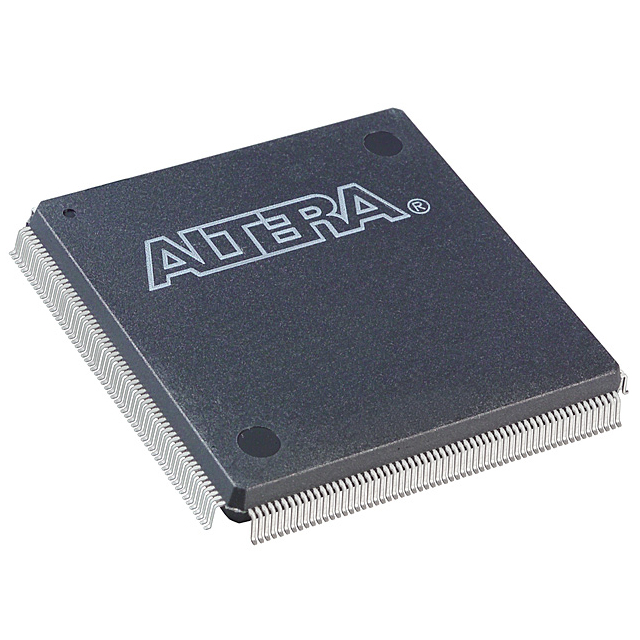
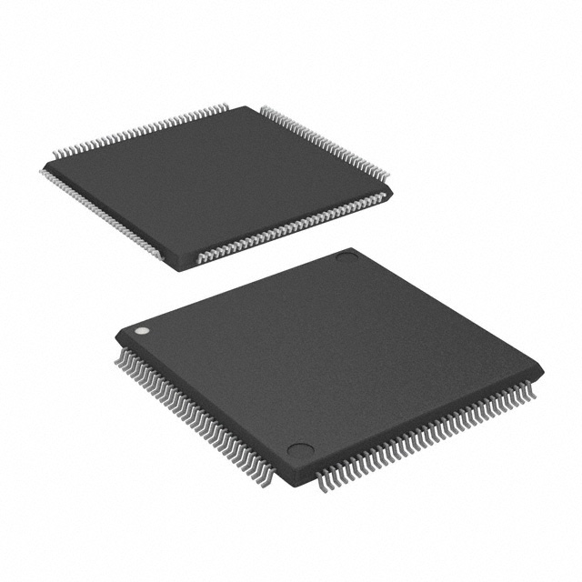
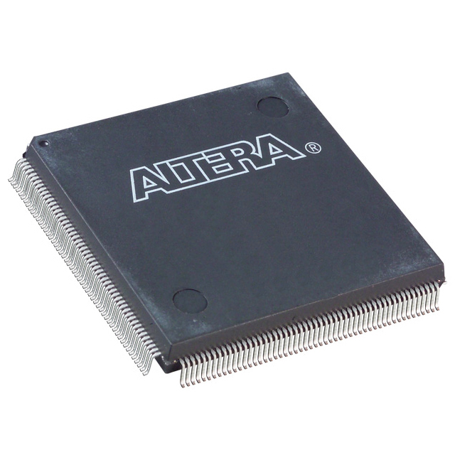
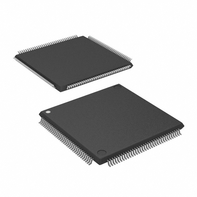
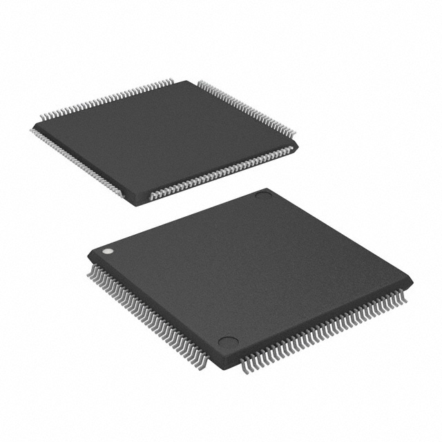
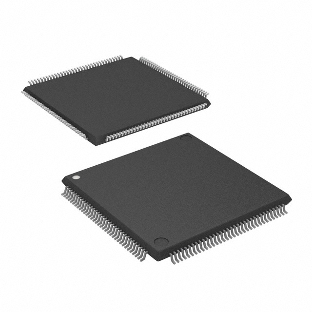
FLEX 6000 Field Programmable Gate Array (FPGA) IC 117 1320 144-LQFP |
|---|---|
| Quantity | 604 Available (as of October 8, 2026) |
| Product Category | Field Programmable Gate Array (FPGA) |
|---|---|
| Manufacturer | Intel |
| Manufacturing Status | Obsolete |
| Manufacturer Standard Lead Time | Contact Us |
| Datasheet |
Specifications & Environmental
| Device Package | 144-TQFP (20x20) | Grade | Commercial | Operating Temperature | 0°C – 85°C | ||
|---|---|---|---|---|---|---|---|
| Package / Case | 144-LQFP | Number of I/O | 117 | Voltage | 4.75 V - 5.25 V | ||
| Mounting Method | Surface Mount | RoHS Compliance | Unknown | REACH Compliance | REACH Unaffected | ||
| Moisture Sensitivity Level | 3 (168 Hours) | Number of LABs/CLBs | 132 | Number of Logic Elements/Cells | 1320 | ||
| Number of Gates | 16000 | ECCN | 3A991D | HTS Code | 8542.39.0001 | ||
| Qualification | N/A |
Overview of EPF6016TC144-2N – FLEX 6000 Field Programmable Gate Array (FPGA) IC 117 1320 144-LQFP
The EPF6016TC144-2N is a FLEX 6000 family FPGA offering a register-rich, look-up table (LUT)-based architecture optimized for low-cost, reprogrammable logic. With 1,320 logic elements and approximately 16,000 typical gates, this device targets prototyping, design testing, and low- to mid-volume replacements for gate-array designs.
Designed for 5.0 V systems, the device comes in a 144-pin LQFP surface-mount package and provides up to 117 I/O pins. Family-level features include OptiFLEX area-efficient architecture, in-circuit reconfigurability, JTAG boundary-scan, and a built-in low-skew clock distribution tree suitable for time-sensitive logic designs.
Key Features
- Core Architecture Register-rich, LUT-based OptiFLEX architecture that improves device area efficiency and supports reconfigurable SRAM-based designs.
- Logic Density 1,320 logic elements and a typical gate count of 16,000 provide a compact footprint for mid-density logic implementations.
- I/O and Pin Control Up to 117 I/O pins with individual tri-state output-enable control and programmable output slew-rate control to manage switching noise and interface timing.
- System-Level Reconfiguration In-circuit reconfigurability (ICR) via an external configuration device or intelligent controller enables field updates and rapid prototyping iterations.
- Built-in Test and Debug IEEE Std. 1149.1 JTAG boundary-scan (BST) circuitry is integrated and available without consuming additional device logic.
- Interconnect and Arithmetic Support FastTrack continuous routing, dedicated carry and cascade chains for high-speed arithmetic and high-fan-in logic functions.
- Package & Mounting 144-LQFP (surface mount) package suitable for standard PCB assembly processes.
- Power and Temperature Supply voltage range 4.75 V to 5.25 V; commercial operating temperature range 0 °C to 85 °C.
- Compliance RoHS compliant.
Typical Applications
- Gate-array replacements and low-volume production Use the EPF6016TC144-2N as a programmable alternative to fixed gate-array designs for reduced NRE and faster time-to-market.
- Prototyping and design validation Reprogrammable SRAM-based logic and in-circuit reconfiguration make it well suited for iterative hardware development and testing.
- PCI 5.0 V system interfaces As a 5.0-V device within the FLEX 6000 family, it aligns with systems that require 5.0-V signaling and compliance with PCI Local Bus Specification environments noted for the family.
- Embedded control and glue logic Mid-density logic resources and up to 117 I/Os support control, interfacing, and glue-logic tasks in complex boards.
Unique Advantages
- Reprogrammable design flexibility: SRAM-based configuration and in-circuit reconfigurability simplify iterative development and field updates without hardware changes.
- Balanced density and I/O: 1,320 logic elements combined with 117 I/Os provide a practical balance for moderate-complexity designs that require ample external connectivity.
- Integrated testability: Built-in JTAG boundary-scan improves board-level test coverage without consuming device logic.
- Clock and routing efficiency: A built-in low-skew clock distribution tree and FastTrack interconnect support predictable timing and efficient routing for synchronous designs.
- Package compatibility and footprint options: Available in the 144-LQFP package with family-level SameFrame pin-compatibility across FLEX 6000 devices, easing board revisions and device scaling.
Why Choose EPF6016TC144-2N?
The EPF6016TC144-2N positions itself as a pragmatic choice for engineers needing a mid-density, reprogrammable FPGA for prototyping, design testing, and low- to mid-volume production. Its OptiFLEX LUT-based architecture, 1,320 logic elements, and family-level system features—such as in-circuit reconfiguration and integrated JTAG—deliver design flexibility and testability while operating within a 4.75 V to 5.25 V supply window.
This device is suitable for designs that require a balance of logic resources, substantial I/O count, and standard commercial temperature operation. It is supported by the FLEX 6000 family design flow and toolset referenced in the product literature, enabling reuse and scalability across similar device densities.
Request a quote or submit an inquiry to receive pricing, availability, and additional technical information for the EPF6016TC144-2N.





















Date Founded: 1968
Headquarters: Santa Clara, California, USA
Employees: 130,000+
Revenue: $54.23 Billion
Certifications and Memberships: ISO9001:2015, ISO14001:2015, ISO17025:2017, ISO27001:2022, ISO45001:2018, ISO50001:2018


