
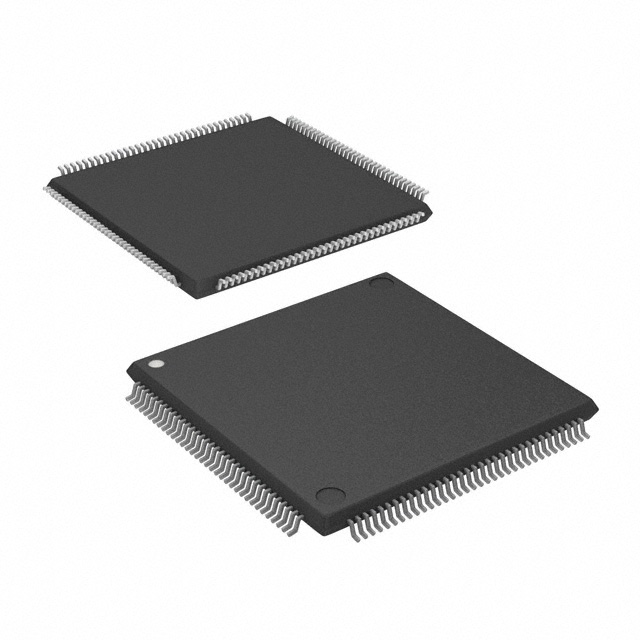
EPF6016TC144-3N
| Part Description |
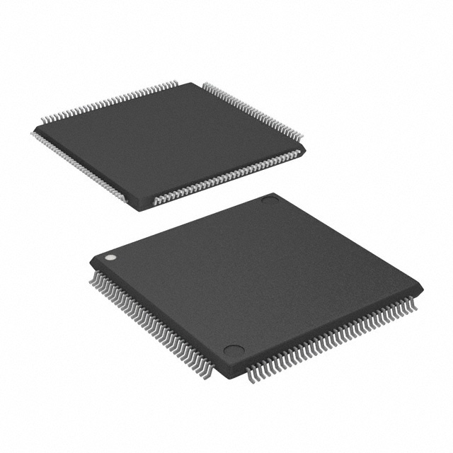
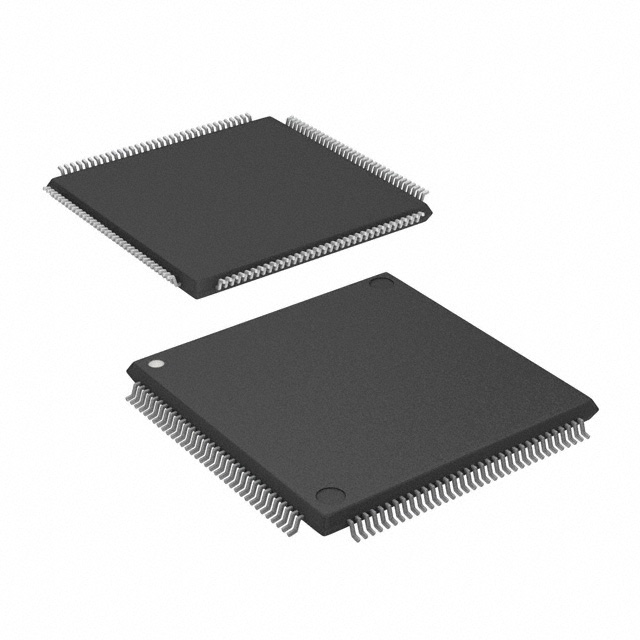
FLEX 6000 Field Programmable Gate Array (FPGA) IC 117 1320 144-LQFP |
|---|---|
| Quantity | 521 Available (as of October 8, 2026) |
| Product Category | Field Programmable Gate Array (FPGA) |
|---|---|
| Manufacturer | Intel |
| Manufacturing Status | Obsolete |
| Manufacturer Standard Lead Time | Contact Us |
| Datasheet |
Specifications & Environmental
| Device Package | 144-TQFP (20x20) | Grade | Commercial | Operating Temperature | 0°C – 85°C | ||
|---|---|---|---|---|---|---|---|
| Package / Case | 144-LQFP | Number of I/O | 117 | Voltage | 4.75 V - 5.25 V | ||
| Mounting Method | Surface Mount | RoHS Compliance | Unknown | REACH Compliance | REACH Unaffected | ||
| Moisture Sensitivity Level | 3 (168 Hours) | Number of LABs/CLBs | 132 | Number of Logic Elements/Cells | 1320 | ||
| Number of Gates | 16000 | ECCN | 3A991D | HTS Code | 8542.39.0001 | ||
| Qualification | N/A |
Overview of EPF6016TC144-3N – FLEX 6000 FPGA, 1,320 Logic Elements, 117 I/O, 144-LQFP
The EPF6016TC144-3N is a FLEX 6000 series field programmable gate array (FPGA) offered in a 144‑pin LQFP surface‑mount package. Based on a register‑rich, look‑up table (LUT) architecture with OptiFLEX area‑efficiency enhancements, this device delivers approximately 16,000 typical gates and 1,320 logic elements for low‑cost, reprogrammable logic implementations.
Targeted at prototyping, design testing and gate‑array replacement use cases, the EPF6016TC144-3N supports in‑circuit reconfigurability and built‑in boundary‑scan (JTAG) for test and programming flexibility. The device operates from 4.75 V to 5.25 V and is specified for commercial temperature use (0 °C to 85 °C).
Key Features
- Core Architecture Register‑rich, LUT‑based OptiFLEX architecture that improves device area efficiency and supports fast logic implementation.
- Logic Capacity Approximately 16,000 typical gates and 1,320 logic elements to implement mid‑density combinational and sequential logic functions.
- I/O and Signal Path 117 available I/O pins with per‑pin tri‑state control and programmable output slew‑rate to help manage switching noise and interface timing.
- Configuration & Test In‑circuit reconfigurability (ICR) via external configuration device or controller and built‑in IEEE‑1149.1 JTAG boundary‑scan circuitry for device programming and board‑level testability.
- System Integration 5.0‑V device family characteristics and system features applicable to PCI Local Bus environments as described for 5.0‑V FLEX 6000 devices.
- Package & Mounting Surface‑mount 144‑LQFP package (supplier device package listed as 144‑TQFP, 20×20) for compact PCB footprint and standard assembly processes.
- Electrical & Environmental Supply voltage range 4.75 V to 5.25 V; commercial grade operation from 0 °C to 85 °C; RoHS compliant.
Typical Applications
- Prototyping & Design Validation Use reprogrammable logic to iterate hardware designs quickly during prototype and validation phases.
- Gate‑Array Replacement Implement mid‑density custom logic and glue‑logic functions as a lower‑cost, reprogrammable alternative to fixed gate‑array devices.
- Peripheral & Bus Interfacing Bridge or control peripheral interfaces where 5.0‑V operation and flexible I/O control are required.
- Board‑Level Test & In‑System Reconfiguration Employ IEEE‑1149.1 JTAG boundary‑scan for production test and use in‑circuit reconfiguration to update logic without board removal.
Unique Advantages
- Reprogrammable Flexibility: In‑circuit reconfigurability allows design changes and firmware updates without hardware swaps, accelerating development cycles.
- Verified Device Family: FLEX 6000 family devices are 100% functionally tested prior to shipment, simplifying production acceptance.
- Efficient Logic Density: OptiFLEX architecture and LUT‑based logic deliver efficient use of silicon for approximately 1,320 logic elements and 16,000 typical gates.
- Built‑In Testability: Integrated JTAG boundary‑scan (IEEE‑1149.1) enables board‑level test and diagnostics without consuming user logic.
- Standard Packaging: 144‑LQFP surface‑mount package offers a compact footprint compatible with common PCB assembly flows.
- Regulatory & Environmental Compliance: RoHS compliance supports environmentally conscious designs and supply requirements.
Why Choose EPF6016TC144-3N?
The EPF6016TC144-3N positions itself as a practical, mid‑density FPGA for teams needing reprogrammable logic with clear testability and system integration features. With approximately 1,320 logic elements, 117 I/O pins and OptiFLEX architecture, it is well suited to prototyping, design validation, and replacing fixed gate‑array logic where iterative development and in‑system updates are valuable.
Its 5 V supply range, commercial temperature rating, and LQFP surface‑mount package make it straightforward to integrate into existing PCB designs while benefiting from the FLEX 6000 family’s development ecosystem and built‑in test features.
If you would like pricing, availability, or to request a formal quote for EPF6016TC144-3N, please submit an inquiry or request a quote through your preferred procurement channel.





















Date Founded: 1968
Headquarters: Santa Clara, California, USA
Employees: 130,000+
Revenue: $54.23 Billion
Certifications and Memberships: ISO9001:2015, ISO14001:2015, ISO17025:2017, ISO27001:2022, ISO45001:2018, ISO50001:2018


