
EPF6016TI144-2
| Part Description |
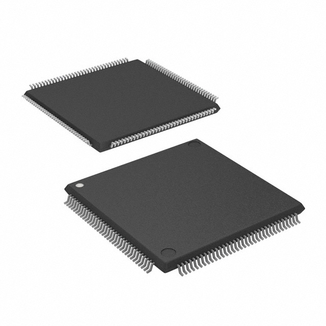
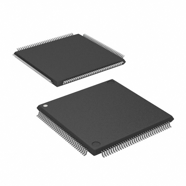
FLEX 6000 Field Programmable Gate Array (FPGA) IC 117 1320 144-LQFP |
|---|---|
| Quantity | 1,460 Available (as of October 8, 2026) |
| Product Category | Field Programmable Gate Array (FPGA) |
|---|---|
| Manufacturer | Intel |
| Manufacturing Status | Obsolete |
| Manufacturer Standard Lead Time | Contact Us |
| Datasheet |
Specifications & Environmental
| Device Package | 144-TQFP (20x20) | Grade | Industrial | Operating Temperature | -40°C – 100°C | ||
|---|---|---|---|---|---|---|---|
| Package / Case | 144-LQFP | Number of I/O | 117 | Voltage | 4.5 V - 5.5 V | ||
| Mounting Method | Surface Mount | RoHS Compliance | RoHS non-compliant | REACH Compliance | REACH Unaffected | ||
| Moisture Sensitivity Level | 3 (168 Hours) | Number of LABs/CLBs | 132 | Number of Logic Elements/Cells | 1320 | ||
| Number of Gates | 16000 | ECCN | 3A991D | HTS Code | 8542.39.0001 | ||
| Qualification | N/A |
Overview of EPF6016TI144-2 – FLEX 6000 FPGA, 1,320 logic elements, 117 I/O, 144‑LQFP
The EPF6016TI144-2 is an Intel FLEX 6000 family field‑programmable gate array (FPGA) offered in a 144‑lead LQFP package. It implements a register‑rich, LUT‑based OptiFLEX architecture that targets low‑cost, reprogrammable logic for prototyping and production systems requiring mid‑density integration.
Key built‑in capabilities include 1,320 logic elements (approximately 16,000 typical gates), 117 general‑purpose I/O pins, support for in‑circuit reconfiguration, and industrial operating range, making it suitable for embedded control and system‑level glue logic where reprogrammability and board‑level I/O density matter.
Key Features
- Core architecture – Register‑rich, LUT‑based OptiFLEX architecture delivering 1,320 logic elements and about 16,000 typical gates for mid‑density logic integration.
- I/O and interfacing – 117 I/O pins providing flexible system interfacing; individual tri‑state output enables and programmable output slew‑rate control are available at the family level.
- Reconfiguration and test – Supports in‑circuit reconfigurability (ICR) and includes built‑in JTAG boundary‑scan (IEEE Std. 1149.1‑1990) for board test and programming without consuming device logic.
- Clock and routing – Built‑in low‑skew clock distribution tree and dedicated carry/cascade chains to support fast arithmetic and high‑fan‑in logic (family‑level features).
- Memory – Total on‑chip RAM bits: 0 (no embedded RAM reported for this device).
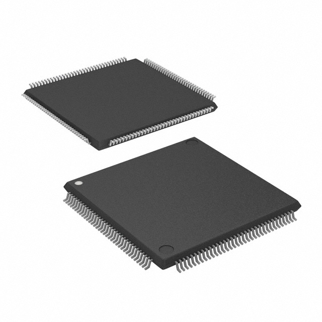
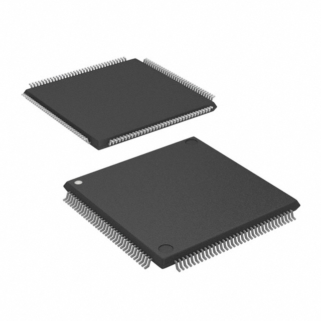
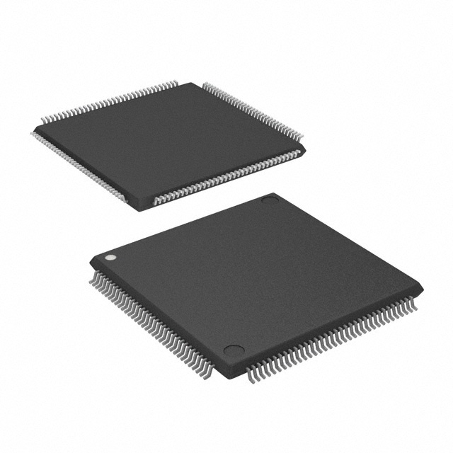
- Package and assembly – Surface‑mount package case: 144‑LQFP; supplier device package listed as 144‑TQFP (20×20).
- Power and temperature – Voltage supply range: 4.5 V to 5.5 V; industrial operating temperature: −40 °C to 100 °C.
- Quality and compliance – Devices are 100% functionally tested prior to shipment; RoHS compliant.
Typical Applications
- Prototyping and development – In‑circuit reconfigurability allows rapid design iteration and functional testing during prototype and validation cycles.
- Embedded control and glue logic – Mid‑density logic resources and 117 I/O pins make the device suitable for consolidating discrete logic, control sequencing, and peripheral interfacing on a single FPGA.
- Industrial systems – Industrial temperature rating and robust packaging support deployment in factory automation, instrumentation, and industrial controller applications.
- Board‑level test and production support – Built‑in JTAG boundary‑scan simplifies board test, programming, and in‑system updates without consuming user logic.
Unique Advantages
- Mid‑density integration: 1,320 logic elements and ~16,000 gates provide a balance of logic capacity and cost for mid‑range designs.
- High I/O count in a compact footprint: 117 I/Os in a 144‑lead LQFP/TQFP package enables dense external interfacing while maintaining a compact board footprint.
- Industrial operating range: Rated for −40 °C to 100 °C, supporting reliable operation in a wide range of ambient conditions.
- Flexible reprogramming and testability: In‑circuit reconfiguration and IEEE‑1149.1 boundary‑scan support reduce development cycle time and simplify field updates and board diagnostics.
- Standards‑oriented supply range: 4.5–5.5 V supply compatibility supports legacy 5.0 V system environments.
- Regulatory and manufacturing readiness: 100% functional testing and RoHS compliance provide traceable manufacturing quality and environmental compliance.
Why Choose EPF6016TI144-2?
The EPF6016TI144-2 positions itself as a practical, reprogrammable solution for engineers who need mid‑density FPGA resources combined with substantial I/O in a compact, surface‑mount package. With 1,320 logic elements, approximately 16,000 gates of logic capacity, and 117 I/Os, it is well suited to consolidate discrete logic, implement custom control functions, and accelerate prototyping efforts while supporting in‑system updates.
Designed for industrial environments and supplied RoHS‑compliant and 100% functionally tested, this FLEX 6000 device is a dependable option for embedded systems, industrial controls, and production boards that require reprogrammability, testability, and a 5 V supply domain.
If you would like pricing, lead‑time, or a formal quote for EPF6016TI144-2, request a quote or submit an inquiry and our team will respond with the details you need.





















Date Founded: 1968
Headquarters: Santa Clara, California, USA
Employees: 130,000+
Revenue: $54.23 Billion
Certifications and Memberships: ISO9001:2015, ISO14001:2015, ISO17025:2017, ISO27001:2022, ISO45001:2018, ISO50001:2018


