
EPF6016TI144-3
| Part Description |
FLEX 6000 Field Programmable Gate Array (FPGA) IC 117 1320 144-LQFP |
|---|---|
| Quantity | 170 Available (as of June 9, 2026) |

| Product Category | Field Programmable Gate Array (FPGA) |
|---|---|
| Manufacturer | Intel |
| Manufacturing Status | Obsolete |
| Manufacturer Standard Lead Time | Contact Us |
| Datasheet |
Specifications & Environmental
| Device Package | 144-TQFP (20x20) | Grade | Industrial | Operating Temperature | -40°C – 100°C | ||
|---|---|---|---|---|---|---|---|
| Package / Case | 144-LQFP | Number of I/O | 117 | Voltage | 4.5 V - 5.5 V | ||
| Mounting Method | Surface Mount | RoHS Compliance | RoHS non-compliant | REACH Compliance | REACH Unaffected | ||
| Moisture Sensitivity Level | 3 (168 Hours) | Number of LABs/CLBs | 132 | Number of Logic Elements/Cells | 1320 | ||
| Number of Gates | 16000 | ECCN | 3A991D | HTS Code | 8542.39.0001 | ||
| Qualification | N/A |
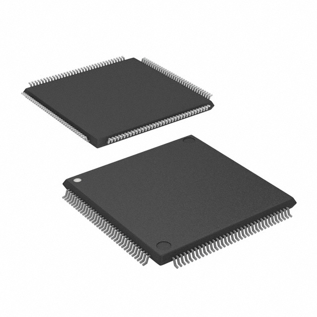
Overview of EPF6016TI144-3 – FLEX 6000 FPGA, 117 I/O, 1,320 logic elements, 144-LQFP
The EPF6016TI144-3 is a FLEX 6000 family programmable logic device from Intel designed as a low-cost, reprogrammable alternative to high-volume gate array designs. It uses a register-rich, look-up table (LUT) based OptiFLEX architecture with reconfigurable SRAM elements to enable rapid design iteration and in-circuit updates.
Targeted for prototyping, design testing and industrial systems, the device combines a compact logic fabric with 117 I/O pins, in-system reconfigurability and industrial-grade operating conditions for robust board- and system-level integration.
Key Features
- Core architecture – Register-rich, LUT-based OptiFLEX architecture for area-efficient programmable logic.
- Logic capacity – Approximately 1,320 logic elements providing a typical equivalent of 16,000 gates for moderate-complexity functions.
- I/O and mixed-voltage support – 117 user I/O pins with MultiVolt I/O interface operation to enable bridging between systems running at different voltages.
- Configuration and test – In-circuit reconfigurability via external configuration device and IEEE 1149.1 (JTAG) boundary-scan circuitry available without consuming device logic; devices are 100% functionally tested prior to shipment.
- Dedicated arithmetic and high-fan-in resources – Dedicated carry and cascade chains for efficient implementation of adders, counters, comparators and high-fan-in logic.
- Clocking – Built-in low-skew clock distribution tree with four low-skew global paths for clock, clear, preset or logic signals.
- Power and supply – Operates from 4.5 V to 5.5 V; low standby current (typical specification less than 0.5 mA).
- Package and thermal – 144-pin LQFP package (supplier device package listed as 144-TQFP, 20×20 mm) with an operating temperature range of −40 °C to 100 °C.
- Standards and compliance – 5.0-V device compatibility with the PCI Local Bus Specification, Revision 2.2; RoHS compliant.
Typical Applications
- Prototyping and design validation – Reconfigurable SRAM-based fabric and in-circuit reconfiguration speed board bring-up and iterative development cycles.
- Gate array replacement – Acts as a programmable alternative to fixed gate arrays for lower-volume or evolving designs.
- PCI-based systems – 5.0-V device compatibility with PCI Local Bus Specification, Revision 2.2 makes the device suitable for PCI interface implementations.
- Mixed-voltage interface and bridging – MultiVolt I/O supports interfacing between different logic voltages in heterogeneous systems.
- Industrial control and embedded systems – Industrial-grade qualification and wide operating temperature range support deployment in factory and instrumentation environments.
Unique Advantages
- In-system reconfigurability: Reprogrammable SRAM elements and in-circuit configuration support enable functional changes without board remanufacture.
- Balanced logic and I/O integration: 1,320 logic elements paired with 117 I/O pins fit applications that require moderate logic density and significant external interfacing.
- Built-in testability: IEEE 1149.1 JTAG boundary-scan support and 100% functional device testing simplify board-level validation and manufacturing test.
- Efficient arithmetic and logic primitives: Dedicated carry and cascade chains reduce routing overhead and improve implementation efficiency for adders, counters and high-fan-in logic.
- Industrial-ready packaging and thermal range: 144-pin LQFP package and −40 °C to 100 °C rating suit demanding environmental requirements.
- Family-level compatibility: FLEX 6000 family pin-compatibility and OptiFLEX architecture help simplify upgrades across device densities and pin counts.
Why Choose EPF6016TI144-3?
The EPF6016TI144-3 provides a pragmatic balance of programmable logic capacity, I/O count and industrial operating range for engineers replacing gate-array designs or accelerating prototype-to-product cycles. Its OptiFLEX LUT-based architecture, dedicated arithmetic resources and in-system reconfiguration capabilities make it suitable for designs that need moderate logic integration with significant external interfacing.
Backed by Intel’s FLEX 6000 family feature set—on-package options, standard compliance for PCI systems and factory-level functional testing—this device delivers a durable, upgradable platform for OEMs and development teams seeking predictable integration and field reprogrammability.
Request a quote or submit an RFQ to receive pricing and availability information for the EPF6016TI144-3.


Date Founded: 1968
Headquarters: Santa Clara, California, USA
Employees: 130,000+
Revenue: $54.23 Billion
Certifications and Memberships: ISO9001:2015, ISO14001:2015, ISO17025:2017, ISO27001:2022, ISO45001:2018, ISO50001:2018


