
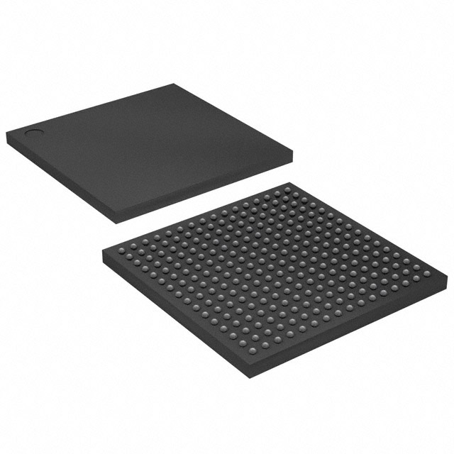
EPF6024ABC256-2
| Part Description |
FLEX 6000 Field Programmable Gate Array (FPGA) IC 218 1960 256-BBGA |
|---|---|
| Quantity | 117 Available (as of June 15, 2026) |

| Product Category | Field Programmable Gate Array (FPGA) |
|---|---|
| Manufacturer | Intel |
| Manufacturing Status | Obsolete |
| Manufacturer Standard Lead Time | Contact Us |
| Datasheet |
Specifications & Environmental
| Device Package | 256-BGA (27x27) | Grade | Commercial | Operating Temperature | 0°C – 85°C | ||
|---|---|---|---|---|---|---|---|
| Package / Case | 256-BBGA | Number of I/O | 218 | Voltage | 3 V - 3.6 V | ||
| Mounting Method | Surface Mount | RoHS Compliance | RoHS non-compliant | REACH Compliance | REACH Unaffected | ||
| Moisture Sensitivity Level | 3 (168 Hours) | Number of LABs/CLBs | 196 | Number of Logic Elements/Cells | 1960 | ||
| Number of Gates | 24000 | ECCN | 3A001A2A | HTS Code | 8542.39.0001 | ||
| Qualification | N/A |
Overview of EPF6024ABC256-2 – FLEX 6000 Field Programmable Gate Array (FPGA) IC 218 1960 256-BBGA
The EPF6024ABC256-2 is a FLEX 6000 programmable logic device offering a register-rich, LUT-based architecture with OptiFLEX area efficiency. It provides 1,960 logic elements and a typical gate count of 24,000, making it suitable for medium-complexity, reconfigurable logic functions in commercial systems.
Designed for prototyping, design validation, and commercial system integration, the device supports in-circuit reconfigurability and a mix of system-level features—enabling flexible I/O interfacing and reliable board-level implementation in a 256-BBGA surface-mount package.
Key Features
- Core architecture Register-rich, look-up table (LUT)-based OptiFLEX architecture that optimizes device area efficiency.
- Logic resources Approximately 1,960 logic elements and a typical gate-equivalent of 24,000 to implement medium-density logic functions.
- I/O and interface flexibility Up to 218 I/O pins with individual tri-state output enable control and programmable output slew-rate to manage switching noise and interface timing.
- Configuration and test Supports in-circuit reconfigurability via an external configuration device or controller and includes built-in JTAG boundary-scan (IEEE 1149.1-1990) circuitry; devices are 100% functionally tested prior to shipment.
- Routing and arithmetic support FastTrack interconnect structure with dedicated carry and cascade chains for efficient arithmetic and high-fan-in logic implementation.
- Clocking and timing Built-in low-skew clock distribution tree and four low-skew global paths to support synchronized system signals.
- Package and mounting 256-ball BGA (256-BBGA, 27×27) surface-mount package for compact board placement and higher pin density.
- Power and operating range Supply voltage range of 3.0 V to 3.6 V with low standby current (typical less than 0.5 mA); commercial operating temperature range 0 °C to 85 °C.
- Design tool support Software design support and automatic place-and-route are provided by the FLEX 6000 development system referenced in the device family documentation.
Typical Applications
- Prototyping and design validation Reconfigurable logic enables rapid iteration and in-circuit reconfiguration during development and test phases.
- Commercial system glue logic Implements custom interface logic, protocol bridging, and glue functions in commercial electronics using its dense I/O and LUT-based resources.
- Mixed-voltage interfacing Flexible I/O controls and programmable slew-rate help when bridging subsystems with differing signaling requirements.
- Arithmetic and control blocks Dedicated carry and cascade chains accelerate adders, counters, and comparator functions in control and signal-processing paths.
Unique Advantages
- Reconfigurable hardware In-circuit reconfigurability lets you update logic without replacing hardware, reducing time-to-market for iterative designs.
- Balanced integration 1,960 logic elements and 218 I/O pins combine to reduce external glue logic and simplify board-level designs.
- Built-in testability On-chip JTAG boundary-scan and 100% functional testing improve board-level debug and manufacturing yield confidence.
- Efficient arithmetic support Dedicated carry and cascade chains streamline implementation of fast adders, counters, and high-fan-in logic without consuming excess routing resources.
- Compact, high-density package 256-BBGA package delivers high pin count in a compact footprint for space-constrained commercial applications.
- Low standby power Typical standby current under 0.5 mA helps minimize idle power in battery-assisted or low-power commercial applications.
Why Choose EPF6024ABC256-2?
The EPF6024ABC256-2 positions itself as a practical, reconfigurable solution for commercial designs that require medium-density logic, substantial I/O capacity, and board-level testability. Its OptiFLEX architecture, dedicated arithmetic chains, and comprehensive I/O controls provide a balanced platform for prototyping, interface logic, and system control functions.
Engineers seeking a programmable logic device with in-circuit reconfiguration, built-in JTAG testing, and supported development tools will find the EPF6024ABC256-2 suited to designs where flexibility, integration, and proven device-level testing are important.
Request a quote or submit an inquiry to begin pricing and availability for the EPF6024ABC256-2.


Date Founded: 1968
Headquarters: Santa Clara, California, USA
Employees: 130,000+
Revenue: $54.23 Billion
Certifications and Memberships: ISO9001:2015, ISO14001:2015, ISO17025:2017, ISO27001:2022, ISO45001:2018, ISO50001:2018


