
EPF6024ABC256-2N
| Part Description |
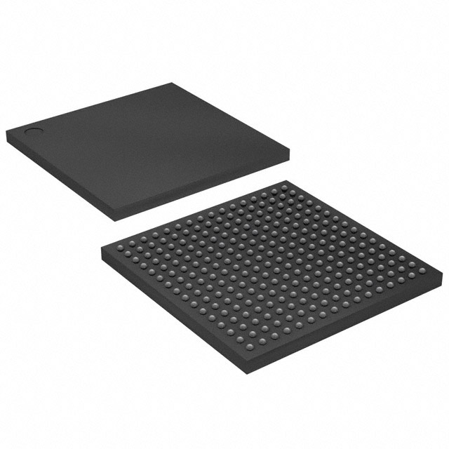
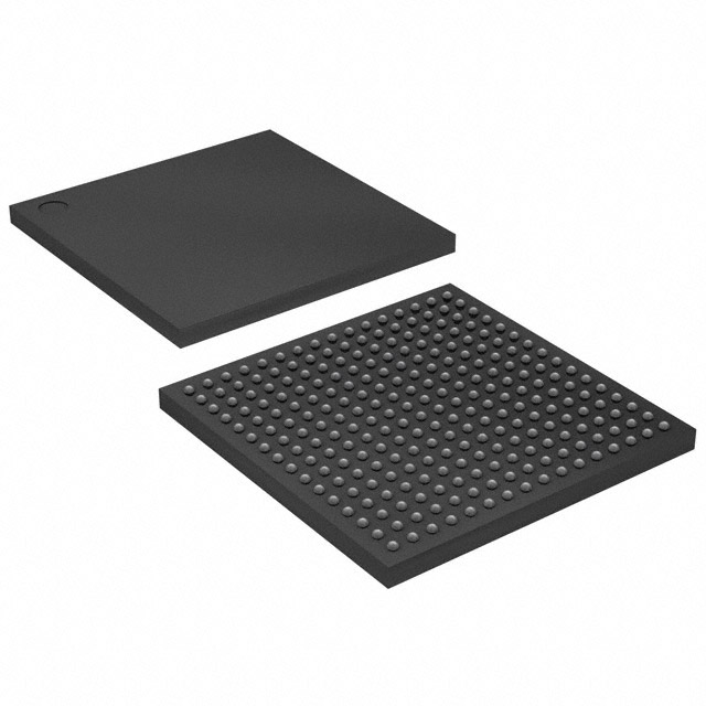
FLEX 6000 Field Programmable Gate Array (FPGA) IC 218 1960 256-BBGA |
|---|---|
| Quantity | 226 Available (as of October 8, 2026) |

| Product Category | Field Programmable Gate Array (FPGA) |
|---|---|
| Manufacturer | Intel |
| Manufacturing Status | Obsolete |
| Manufacturer Standard Lead Time | Contact Us |
| Datasheet |
Specifications & Environmental
| Device Package | 256-BGA (27x27) | Grade | Commercial | Operating Temperature | 0°C – 85°C | ||
|---|---|---|---|---|---|---|---|
| Package / Case | 256-BBGA | Number of I/O | 218 | Voltage | 3 V - 3.6 V | ||
| Mounting Method | Surface Mount | RoHS Compliance | Unknown | REACH Compliance | REACH Unaffected | ||
| Moisture Sensitivity Level | 3 (168 Hours) | Number of LABs/CLBs | 196 | Number of Logic Elements/Cells | 1960 | ||
| Number of Gates | 24000 | ECCN | 3A001A2A | HTS Code | 8542.39.0001 | ||
| Qualification | N/A |
Overview of EPF6024ABC256-2N – FLEX 6000 Field Programmable Gate Array (FPGA) IC 218 1960 256-BBGA
The EPF6024ABC256-2N is a FLEX 6000 family FPGA from Intel designed as a low-cost, reprogrammable alternative to fixed gate-array implementations. Built on a register-rich, look-up table (LUT) OptiFLEX architecture with reconfigurable SRAM elements, this device targets prototyping, design testing, and low-volume production where fast design changes and in-circuit updates are required.
Key on-board resources include approximately 1,960 logic elements and support for up to 24,000 typical gates, with 218 I/O pins in a 256-ball BGA package. The device operates from a 3.0 V to 3.6 V supply and meets commercial temperature requirements (0 °C to 85 °C).
Key Features
- Core Architecture Register-rich, LUT-based OptiFLEX architecture providing approximately 1,960 logic elements and a typical gate-equivalent of 24,000 for flexible combinational and sequential logic implementation.
- I/O and Interface Up to 218 I/O pins supported; MultiVolt I/O operation available at the family level to bridge systems operating at differing voltages and provide flexible interfacing options.
- System-Level Reconfigurability Supports in-circuit reconfiguration via an external configuration device or intelligent controller, enabling field updates and design iteration without socket removal.
- On-Chip Routing and Arithmetic Support FastTrack interconnect structure with dedicated carry and cascade chains for efficient arithmetic functions (adders, counters, comparators) and high-fan-in logic.
- Built-in Test and Clocking IEEE 1149.1 JTAG boundary-scan test circuitry is available without consuming user logic; low-skew global clock distribution and four global paths for clock/clear/preset or logic signals.
- Package and Mounting 256-ball BGA (256-BBGA / 256-BGA 27×27) surface-mount package offering a compact footprint and SameFrame pin-compatibility across FLEX 6000 devices in similar packages.
- Supply and Temperature Supply voltage range of 3.0 V to 3.6 V and commercial-grade operating temperature from 0 °C to 85 °C.
- Regulatory RoHS compliant.
Typical Applications
- Gate-array replacement: Use the EPF6024ABC256-2N as a cost-effective, reprogrammable substitute for low- to mid-volume gate-array designs where rapid changes are anticipated.
- Prototyping and design testing: Ideal for iterative hardware development and validation thanks to reprogrammable SRAM elements and in-circuit reconfiguration capability.
- Mixed-voltage interface logic: Implement bridging and protocol translation between subsystems operating at different I/O voltages using the device’s MultiVolt I/O features.
- High-speed arithmetic and control: Leverage dedicated carry and cascade chains for fast adders, counters, and comparator implementations in embedded control logic.
Unique Advantages
- Reprogrammable flexibility: In-circuit reconfiguration enables updates and functional changes without board rework, accelerating development cycles and field maintenance.
- Compact logic density: Approximately 1,960 logic elements and 24,000 typical gates provide significant implementation capability in a single 256-BGA package.
- Extensive I/O count: 218 available I/O pins support complex interfacing needs while maintaining a compact BGA footprint.
- Built-in testability: IEEE 1149.1 JTAG boundary-scan circuitry supports board-level test without consuming user logic resources.
- Dedicated arithmetic chains: Hardware carry and cascade chains simplify and accelerate implementation of arithmetic and high-fan-in logic functions.
- Tool and IP ecosystem: Family-level design support includes common HDL and netlist flows and compatibility with standard EDA tools for efficient design entry and synthesis.
Why Choose EPF6024ABC256-2N?
The EPF6024ABC256-2N is positioned for designers needing a commercially graded, reprogrammable logic device that balances density, I/O richness, and system-level configurability. Its OptiFLEX architecture, dedicated arithmetic chains, and in-circuit reconfiguration make it well suited to prototyping, gate-array replacement, and mixed-voltage interface logic.
With a compact 256-BGA package, support for 3.0–3.6 V supply operation, and RoHS compliance, this device offers a practical option for commercial embedded designs that require frequent design iteration and flexible integration into existing PCB footprints.
Request a quote or submit a purchase inquiry to obtain pricing and availability for EPF6024ABC256-2N.




















Date Founded: 1968
Headquarters: Santa Clara, California, USA
Employees: 130,000+
Revenue: $54.23 Billion
Certifications and Memberships: ISO9001:2015, ISO14001:2015, ISO17025:2017, ISO27001:2022, ISO45001:2018, ISO50001:2018


