
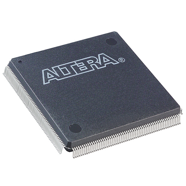
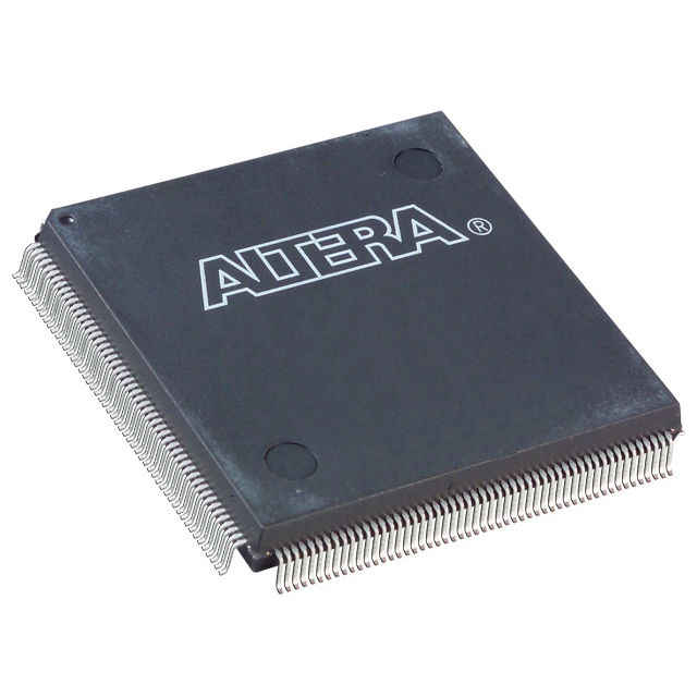
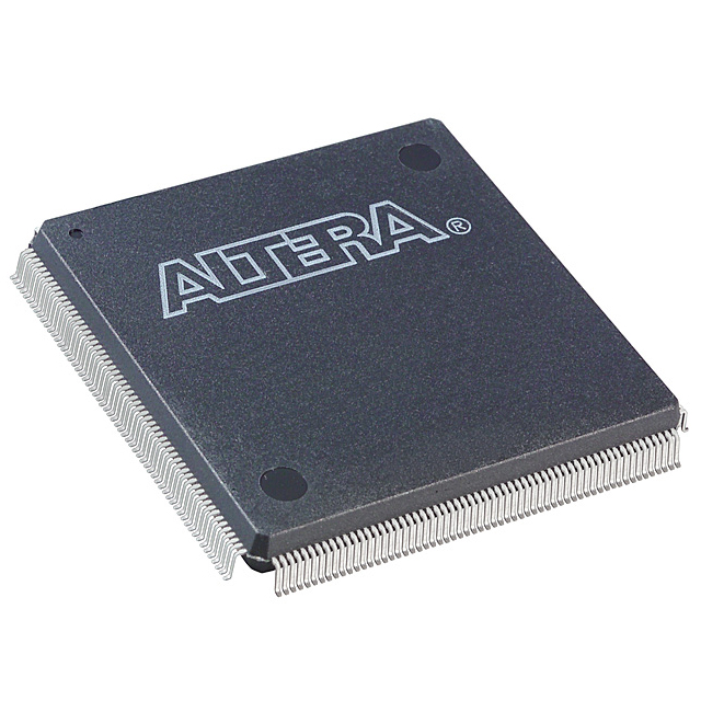
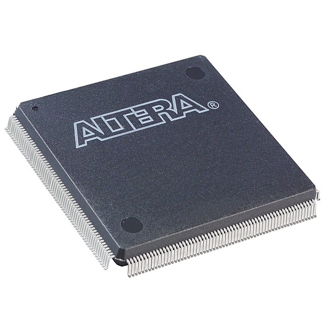
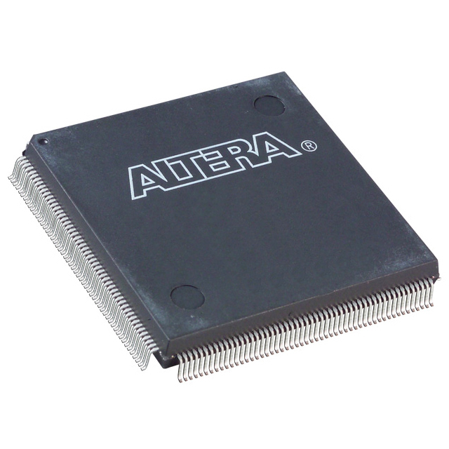
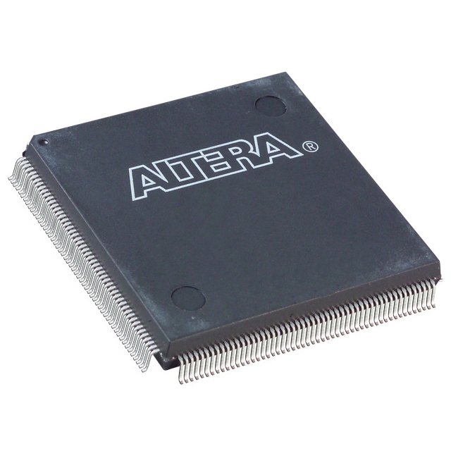
EPF81188AQC240-4
| Part Description |
FLEX 8000 Field Programmable Gate Array (FPGA) IC 184 1008 240-BFQFP |
|---|---|
| Quantity | 460 Available (as of October 8, 2026) |
| Product Category | Field Programmable Gate Array (FPGA) |
|---|---|
| Manufacturer | Intel |
| Manufacturing Status | Obsolete |
| Manufacturer Standard Lead Time | Contact Us |
| Datasheet |
Specifications & Environmental
| Device Package | 240-PQFP (32x32) | Grade | Commercial | Operating Temperature | 0°C – 70°C | ||
|---|---|---|---|---|---|---|---|
| Package / Case | 240-BFQFP | Number of I/O | 184 | Voltage | 4.75 V - 5.25 V | ||
| Mounting Method | Surface Mount | RoHS Compliance | Unknown | REACH Compliance | REACH Unaffected | ||
| Moisture Sensitivity Level | 3 (168 Hours) | Number of LABs/CLBs | 126 | Number of Logic Elements/Cells | 1008 | ||
| Number of Gates | 12000 | ECCN | 3A001A2A | HTS Code | 8542.39.0001 | ||
| Qualification | N/A |
Overview of EPF81188AQC240-4 – FLEX 8000 Field Programmable Gate Array (FPGA) IC
The EPF81188AQC240-4 is a FLEX 8000 family FPGA offered by Intel, provided in a 240-pin BFQFP package. It combines a fine-grained logic architecture of 1,008 logic elements with a high I/O count to target mid-range programmable logic applications requiring substantial register resources and predictable interconnect.
Designed for commercial-temperature systems, this device supports 5.0 V core operation (4.75 V to 5.25 V supply range) and provides a balance of integration, I/O density, and low-power standby behavior for bus interfaces, data transformation, and control applications.
Key Features
- Core architecture FLEX family architecture with compact 4-input look-up tables and programmable registers for register-rich logic implementation.
- Logic density 1,008 logic elements and approximately 12,000 usable gates, enabling mid-range integration for controllers and glue-logic functions.
- Logic array resources 126 logic array blocks to structure logic and registers for predictable placement and routing.
- I/O capability 184 user I/O pins for high pin-count system integration and multi-bus interfaces.
- Power and voltage Operates from 4.75 V to 5.25 V; family-level MultiVolt I/O enables device core to run at 5.0 V while supporting 5.0 V and 3.3 V logic levels on I/O pins.
- Low-power standby Family-level typical standby current specification of 0.5 mA or less.
- System-level features Supports in-circuit reconfigurability via external configuration devices or intelligent controllers; family includes PCI Local Bus Specification, Revision 2.2 compliance for 5.0 V operation (series-level).
- Fast, predictable interconnect Series FastTrack continuous routing structure and dedicated arithmetic/cascade chains to accelerate adders, counters, comparators, and high-fan-in logic (series-level).
- Packaging 240-BFQFP package (supplier device package listed as 240-PQFP 32×32) in surface-mount form factor for high-pin-count board designs.
- Commercial temperature grade Rated for 0 °C to 70 °C operation and RoHS compliant.
- On-chip memory No on-chip RAM bits (Total Ram Bits: 0), for applications that depend on distributed registers and LUT-based logic rather than embedded block RAM.
Typical Applications
- Digital signal processing (DSP) Register-rich logic and dedicated arithmetic resources make the device suitable for datapath manipulation and signal conditioning tasks within mid-range DSP pipelines.
- Bus interfaces and controllers High I/O count and PCI-series compliance (for 5.0 V operation) support implementation of parallel bus bridges, interface controllers, and glue logic between TTL/legacy subsystems.
- Coprocessor and acceleration logic Use as custom coprocessor or accelerator functions where compact LUT-based logic and abundant registers reduce external component count.
- TTL integration and system glue MultiVolt I/O compatibility and 184 I/O pins facilitate integration with 5.0 V and 3.3 V TTL/CMOS devices for system-level interfacing.
- High-pin-count multi-bus aggregation 240-pin package enables consolidation of multiple 32-bit buses or multiple parallel interfaces into a single device for board-level simplification.
Unique Advantages
- Balanced mid-range density: 1,008 logic elements and ~12,000 gates provide a practical compromise between integration and cost for mid-complexity designs.
- High I/O connectivity: 184 user I/O pins support dense external interfacing without expanding to larger, more costly packages.
- 5 V supply compatibility: Operation across 4.75 V–5.25 V and family-level MultiVolt I/O support streamline integration into legacy 5.0 V systems while accommodating 3.3 V signaling at the I/O.
- Surface-mount 240-pin package: 240-BFQFP/240-PQFP (32×32) packaging provides a compact, manufacturable footprint for high-pin-count designs.
- Commercial-grade reliability: Rated for 0 °C–70 °C operation and RoHS compliant to meet standard commercial product requirements.
- Low standby power: Family-level standby current of 0.5 mA or less helps reduce system idle power consumption.
Why Choose EPF81188AQC240-4?
The EPF81188AQC240-4 positions itself as a practical FLEX 8000 family FPGA for designers who need mid-range logic capacity, substantial I/O, and 5 V system compatibility. With 1,008 logic elements, 184 I/O pins, and a 240-pin surface-mount package, it is well suited to bus-centric designs, interface consolidation, and register-heavy logic implementations where embedded RAM is not required.
Backed by the FLEX 8000 family architecture and series-level features such as in-circuit reconfigurability, dedicated arithmetic chains, and predictable routing, this device offers a clear migration and development path for commercial applications that demand reliable, programmable logic integration.
Request a quote or submit an availability inquiry to start specifying EPF81188AQC240-4 for your next design.
























Date Founded: 1968
Headquarters: Santa Clara, California, USA
Employees: 130,000+
Revenue: $54.23 Billion
Certifications and Memberships: ISO9001:2015, ISO14001:2015, ISO17025:2017, ISO27001:2022, ISO45001:2018, ISO50001:2018


