
M1A3P1000-1FGG484
| Part Description |
ProASIC3 Field Programmable Gate Array (FPGA) IC 300 147456 484-BGA |
|---|---|
| Quantity | 160 Available (as of June 15, 2026) |

| Product Category | Field Programmable Gate Array (FPGA) |
|---|---|
| Manufacturer | Microchip Technology |
| Manufacturing Status | Active |
| Manufacturer Standard Lead Time | 18 Weeks |
| Datasheet |
Specifications & Environmental
| Device Package | 484-FPBGA (23x23) | Grade | Commercial | Operating Temperature | 0°C – 85°C | ||
|---|---|---|---|---|---|---|---|
| Package / Case | 484-BGA | Number of I/O | 300 | Voltage | 1.425 V - 1.575 V | ||
| Mounting Method | Surface Mount | RoHS Compliance | ROHS3 Compliant | REACH Compliance | REACH Unaffected | ||
| Moisture Sensitivity Level | 3 (168 Hours) | Number of LABs/CLBs | 24576 | Number of Logic Elements/Cells | 24576 | ||
| Number of Gates | 1000000 | ECCN | 3A991D | HTS Code | 8542.39.0001 | ||
| Qualification | N/A | Total RAM Bits | 147456 |
Overview of M1A3P1000-1FGG484 – ProASIC3 Field Programmable Gate Array (FPGA) IC
The M1A3P1000-1FGG484 is a ProASIC3 Flash-based FPGA in a 484-BGA package designed for commercial applications requiring reprogrammable logic, significant I/O capacity, and on-chip embedded memory. Built for designs that need up to 24,576 logic elements and one million equivalent gates, this device targets mid- to high-density FPGA applications where low power, single-chip integration and flexible I/O are important.
This surface-mount device offers 300 user I/Os, approximately 147,456 bits of embedded RAM, and a narrow core supply range (1.425 V to 1.575 V), making it suitable for compact, power-conscious designs that must operate across a commercial temperature range (0 °C to 85 °C).
Key Features
- Logic Capacity 24,576 logic elements (equivalent CLBs) and approximately 1,000,000 system gates enable mid- to high-density logic implementations.
- Embedded Memory Approximately 147,456 bits of on-chip RAM for data buffering, FIFOs, and small embedded memory requirements.
- Rich I/O Up to 300 user I/Os provided in the 484-BGA package to support wide peripheral and bus connectivity.
- Flash-Based Reprogrammability Nonvolatile, reprogrammable flash architecture retains designs when powered off and supports in-system updates.
- Security and In-System Programming Series-level features include on-chip AES-based decryption for secure ISP and FlashLock protection to safeguard FPGA contents.
- Power and Voltage Core supply specified at 1.425 V to 1.575 V (1.5 V class operation) for low-power operation; supports mixed I/O voltage operation as part of the family architecture.
- Clocking Clock conditioning and PLL capabilities are available within the ProASIC3 family architecture to support flexible clock management.
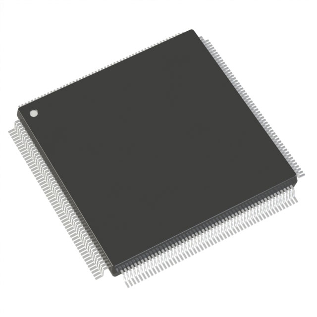
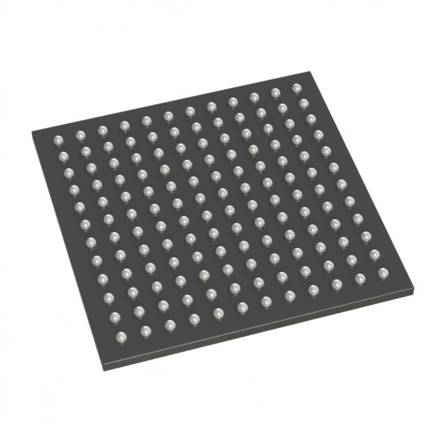
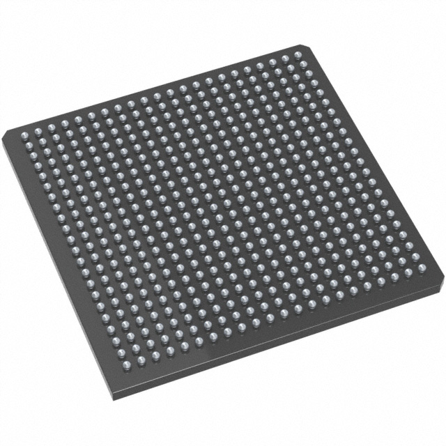
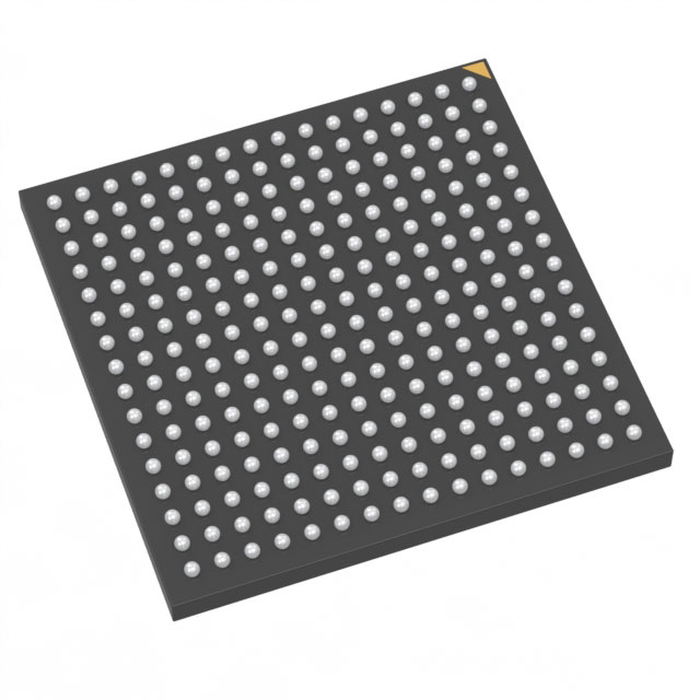
- Package & Assembly 484-BGA (supplier device package 484-FPBGA, 23 × 23 mm) surface-mount package suitable for compact PCB footprints.
- Operating Range & Compliance Commercial grade operation from 0 °C to 85 °C and RoHS-compliant device construction.
Typical Applications
- Consumer Electronics Implement control logic, user interfaces, and protocol bridging in portable or battery-assisted products where low-power, nonvolatile FPGA behavior is advantageous.
- Communications & Networking Use as a mid-density logic engine for protocol conversion, packet buffering, and timing control leveraging abundant I/O and embedded RAM.
- Industrial Automation (Commercial Equipment) Control and interface functions in commercial automation systems that operate within a 0 °C to 85 °C range and require reprogrammable logic.
- Instrumentation & Test Custom signal processing, gating, and timing functions that benefit from on-chip memory and flexible clock conditioning.
Unique Advantages
- High Logic Density: Delivers 24,576 logic elements and 1,000,000 system gates to implement complex designs without moving to larger form factors.
- Significant I/O Count: 300 user I/Os in a 484-BGA provide broad connectivity for multi-channel interfaces and mixed-signal front ends.
- Nonvolatile, Reprogrammable: Flash-based architecture retains programmed designs when power is removed and enables in-system reprogramming for field updates.
- Compact, Surface-Mount Package: The 23 × 23 mm 484-FPBGA package supports dense PCB layouts while maintaining extensive I/O and memory resources.
- Commercial Temperature Suitability: Rated for 0 °C to 85 °C to match commercial-grade product deployment and testing environments.
- Regulatory Compliance: RoHS-compliant construction supports current environmental requirements for commercial electronics.
Why Choose M1A3P1000-1FGG484?
The M1A3P1000-1FGG484 balances substantial logic resources, a high I/O count, and on-chip memory in a compact 484-BGA package, providing a versatile platform for commercial electronic designs that demand reprogrammability and low-power operation. Its flash-based architecture and family-level security features make it suitable for applications that require retained configuration and controlled in-system updates.
This device is well suited to engineers and product teams developing mid- to high-density FPGA solutions who need a single-chip, reprogrammable option with broad I/O and embedded memory while maintaining a commercial operating temperature range and RoHS compliance.
Request a quote or submit a product inquiry to get pricing, availability, and additional technical support for M1A3P1000-1FGG484.


Date Founded: 1989
Headquarters: Chandler, Arizona, USA
Employees: 22,000+
Revenue: $8.349 Billion
Certifications and Memberships: ISO9001:2015, IATF16949:2016, AS 9100D


