
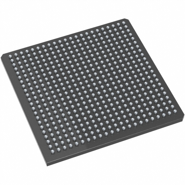
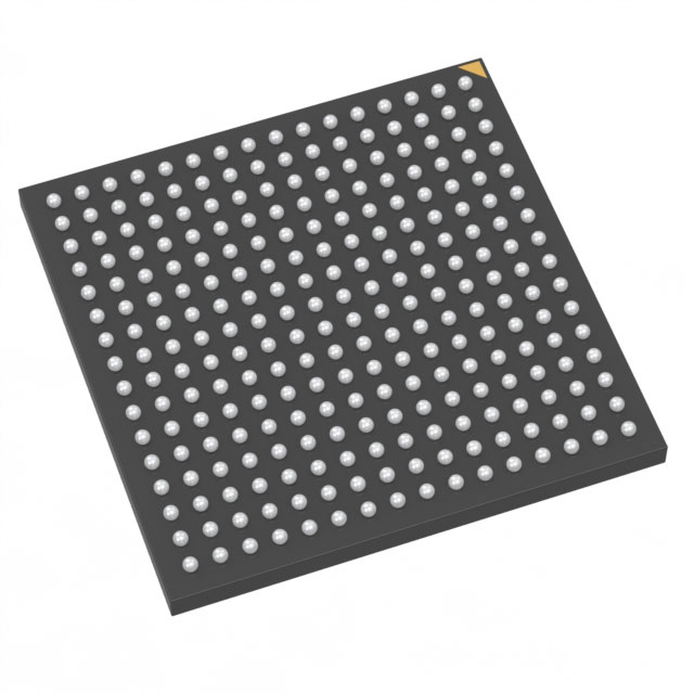
M1A3P1000-1FGG484I
| Part Description |
ProASIC3 Field Programmable Gate Array (FPGA) IC 300 147456 484-BGA |
|---|---|
| Quantity | 472 Available (as of June 18, 2026) |
| Product Category | Field Programmable Gate Array (FPGA) |
|---|---|
| Manufacturer | Microchip Technology |
| Manufacturing Status | Active |
| Manufacturer Standard Lead Time | 18 Weeks |
| Datasheet |
Specifications & Environmental
| Device Package | 484-FPBGA (23x23) | Grade | Industrial | Operating Temperature | -40°C – 100°C | ||
|---|---|---|---|---|---|---|---|
| Package / Case | 484-BGA | Number of I/O | 300 | Voltage | 1.425 V - 1.575 V | ||
| Mounting Method | Surface Mount | RoHS Compliance | ROHS3 Compliant | REACH Compliance | REACH Unaffected | ||
| Moisture Sensitivity Level | 3 (168 Hours) | Number of LABs/CLBs | 24576 | Number of Logic Elements/Cells | 24576 | ||
| Number of Gates | 1000000 | ECCN | 3A991D | HTS Code | 8542.39.0001 | ||
| Qualification | N/A | Total RAM Bits | 147456 |
Overview of M1A3P1000-1FGG484I – ProASIC3 Field Programmable Gate Array (FPGA) IC, 300 I/O, 484-BGA
The M1A3P1000-1FGG484I is a ProASIC3 nano reprogrammable, nonvolatile FPGA from Microchip Technology. It combines a high logic capacity with on-chip embedded RAM and flash-based nonvolatile storage to support instant-on, secure FPGA designs.
Designed for applications where performance, integration and low power matter, this device offers 24,576 logic elements, 300 user I/Os, and an industrial operating range for use in portable, consumer and industrial systems.
Key Features
- Logic Capacity — 24,576 logic elements (VersaTiles/LEs) delivering a programmable fabric equivalent to 1,000,000 system gates for complex control and data-path logic.
- Embedded Memory — 147,456 bits of on-chip RAM and internal FlashROM resources for user nonvolatile storage and SRAM/FIFO requirements.
- High I/O Count & Mixed-Voltage Support — 300 user I/Os with support for mixed I/O voltages and bank-selectable I/O voltages to interface directly with multiple peripheral voltage domains.
- Security and In-System Programming — Series-level support for AES-128 ISP and FlashLock designed to protect programmed contents and enable secure in-system updates.
- Clocking and Timing — Configurable clock conditioning circuitry (CCCs) with integrated PLL options for phase shift, multiply/divide and frequency conditioning suitable for varied clocking needs.
- Power and Voltage — Core supply operation specified from 1.425 V to 1.575 V and architecture-level low-power characteristics suitable for power-sensitive designs.
- Package and Mounting — 484-ball FPBGA package (23 × 23) in surface-mount configuration, optimized for dense board layouts.
- Industrial Temperature Range — Rated for operation from −40 °C to 100 °C, supporting robust performance in industrial environments.
- Standards & I/O Features — Single-ended I/O standards and features from the series including selectable Schmitt trigger inputs, programmable slew rate and drive strength, and JTAG boundary-scan support.
Typical Applications
- Consumer & Portable Electronics — Implement control logic, user interfaces, and glue logic in compact, low-power portable devices that benefit from instant-on nonvolatile FPGA operation.
- Battery-Backed Systems — Use on-chip Flash and low-power core operation to maintain configuration and reduce power draw in battery-backed applications.
- Industrial Control — Leverage the industrial temperature rating and high I/O count for sensor interfacing, I/O aggregation, and real-time control tasks in factory and process automation.
- Secure In-System Programmable Designs — Deploy devices requiring secure firmware updates and IP protection using the series-level AES ISP and FlashLock features.
Unique Advantages
- Reprogrammable Nonvolatile Fabric: Flash-based configuration retains designs when powered off and enables instant-on behavior to simplify system boot.
- High Integration: Large logic element count and substantial on-chip RAM reduce external component count and simplify board-level design.
- Flexible I/O Interfacing: 300 I/Os with mixed-voltage support and bank selection enable direct connection to diverse peripheral voltages without level shifters.
- Secure Update Capability: AES-128 in-system programming and FlashLock provide mechanisms for protected updates and IP protection.
- Industrial Robustness: Surface-mount 484-FPBGA package and −40 °C to 100 °C operating range support deployment in demanding environments.
Why Choose M1A3P1000-1FGG484I?
The M1A3P1000-1FGG484I positions itself as a versatile, secure and low-power FPGA option within the ProASIC3 nano family. Its combination of 24,576 logic elements, substantial on-chip RAM, and 300 user I/Os delivers a balanced platform for designers seeking high integration and reliable operation across industrial and portable applications.
This device is well suited to teams that need nonvolatile, reprogrammable logic with secure in-system update capability, flexible I/O voltage support, and a package footprint optimized for dense PCBs. The industrial temperature rating and surface-mount 484-FPBGA package support long-term deployment in a wide range of systems.
Request a quote or submit an inquiry to check availability and pricing for the M1A3P1000-1FGG484I and to discuss how it can fit into your next design.


Date Founded: 1989
Headquarters: Chandler, Arizona, USA
Employees: 22,000+
Revenue: $8.349 Billion
Certifications and Memberships: ISO9001:2015, IATF16949:2016, AS 9100D


