
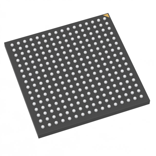
M1A3P250-1FGG144
| Part Description |
ProASIC3 Field Programmable Gate Array (FPGA) IC 97 36864 144-LBGA |
|---|---|
| Quantity | 858 Available (as of June 15, 2026) |

| Product Category | Field Programmable Gate Array (FPGA) |
|---|---|
| Manufacturer | Microchip Technology |
| Manufacturing Status | Active |
| Manufacturer Standard Lead Time | 18 Weeks |
| Datasheet |
Specifications & Environmental
| Device Package | 144-FPBGA (13x13) | Grade | Commercial | Operating Temperature | 0°C – 85°C | ||
|---|---|---|---|---|---|---|---|
| Package / Case | 144-LBGA | Number of I/O | 97 | Voltage | 1.425 V - 1.575 V | ||
| Mounting Method | Surface Mount | RoHS Compliance | ROHS3 Compliant | REACH Compliance | REACH Unaffected | ||
| Moisture Sensitivity Level | 3 (168 Hours) | Number of LABs/CLBs | 6144 | Number of Logic Elements/Cells | 6144 | ||
| Number of Gates | 250000 | ECCN | 3A991D | HTS Code | 8542.39.0001 | ||
| Qualification | N/A | Total RAM Bits | 36864 |
Overview of M1A3P250-1FGG144 – ProASIC3 FPGA, 97 I/Os, 36,864-bit RAM, 144-LBGA
The M1A3P250-1FGG144 is a ProASIC3 Field Programmable Gate Array (FPGA) IC offering a balance of logic capacity, embedded memory and I/O in a compact surface-mount package. Architected for applications that require reprogrammable logic, the device integrates 6,144 logic elements with approximately 36,864 bits of on-chip RAM and 97 user I/Os.
Key device attributes include a 144-LBGA package (supplier device package: 144-FPBGA 13×13), a supply voltage range of 1.425 V to 1.575 V, commercial temperature grading (0 °C to 85 °C), and RoHS compliance—making it suitable for a wide range of commercial embedded designs.
Key Features
- Core Logic 6,144 logic elements (cells) providing a programmable fabric capable of implementing custom digital functions and finite-state logic.
- On-Chip Memory Approximately 36,864 bits of embedded RAM to support data buffering, small FIFOs and local storage for implemented logic.
- I/O Density 97 user I/Os to interface with peripherals, sensors, and system buses while minimizing external glue logic.
- Design Capacity Equivalent to 250,000 gates, enabling moderate-density logic integration within a single FPGA device.
- Power and Supply Operates from a defined core supply range of 1.425 V to 1.575 V to match system power rails and voltage planning.
- Package & Mounting 144-LBGA package (supplier device package: 144-FPBGA 13×13) in a surface-mount form factor for compact PCB integration.
- Temperature & Grade Commercial grade device rated for 0 °C to 85 °C operation.
- Regulatory RoHS compliant.
Typical Applications
- Embedded Control Implement custom control logic and protocol bridges using the device’s 6,144 logic elements and available I/O resources.
- Signal Conditioning and Processing Local buffering and preprocessing of data streams using on-chip RAM and programmable logic before handoff to other system elements.
- Interface Bridging Create custom bus adapters or I/O expanders leveraging 97 user I/Os to connect diverse peripherals and sensors.
- Prototyping and Low- to Mid-Volume Production Use the reprogrammable fabric for iterative development and deployment in commercial-grade electronics within the 0 °C–85 °C range.
Unique Advantages
- Balanced Integration: Combines 6,144 logic elements, approximately 36,864 bits of embedded RAM and 97 I/Os in a single device to reduce external components and simplify board-level design.
- Compact Package: 144-LBGA (144-FPBGA 13×13) surface-mount package enables high-density PCB layouts while providing adequate I/O accessibility.
- Defined Power Envelope: Narrow supply range (1.425 V–1.575 V) simplifies power-supply selection and voltage regulation design.
- Commercial Temperature Rating: Rated for 0 °C to 85 °C operation to match typical commercial electronics deployment scenarios.
- RoHS Compliant: Meets RoHS requirements for lead-free manufacturing and supply-chain compliance.
- Moderate Gate Count: 250,000 gates suitable for designs that require meaningful logic density without moving to higher-end FPGA classes.
Why Choose M1A3P250-1FGG144?
The M1A3P250-1FGG144 delivers a practical combination of logic capacity, on-chip memory and I/O count in a compact 144-LBGA surface-mount package. Its defined supply-voltage window and commercial temperature grade make it a reliable choice for commercial embedded applications that need reprogrammable logic with moderate integration density.
This device is well suited to designers looking to consolidate discrete logic, implement custom interfaces, or prototype control and signal-processing tasks with a single, RoHS-compliant FPGA. The combination of logic elements, embedded RAM and substantial I/O support provides design headroom while keeping BOM and board area considerations in mind.
Request a quote or submit a parts request to obtain pricing and availability for the M1A3P250-1FGG144. Our team can provide lead-time information and assist with volume inquiries.


Date Founded: 1989
Headquarters: Chandler, Arizona, USA
Employees: 22,000+
Revenue: $8.349 Billion
Certifications and Memberships: ISO9001:2015, IATF16949:2016, AS 9100D


