
M1A3PE1500-FGG676
| Part Description |
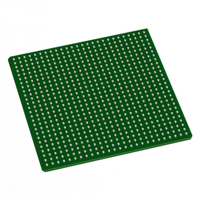
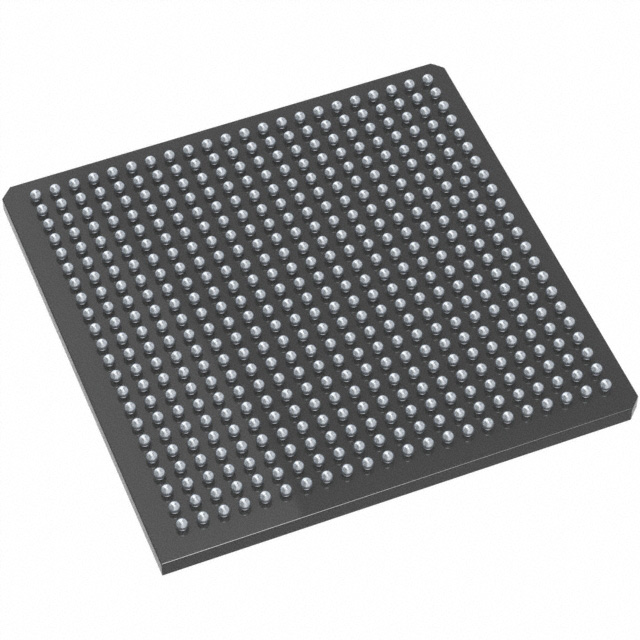
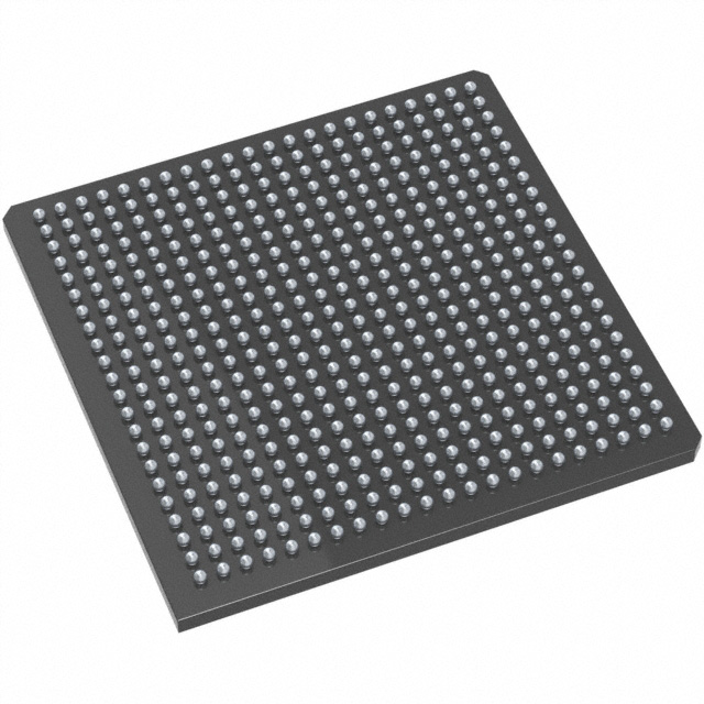
ProASIC3E Field Programmable Gate Array (FPGA) IC 444 276480 676-BGA |
|---|---|
| Quantity | 716 Available (as of October 8, 2026) |
| Product Category | Field Programmable Gate Array (FPGA) |
|---|---|
| Manufacturer | Microchip Technology |
| Manufacturing Status | Active |
| Manufacturer Standard Lead Time | 12 Weeks |
| Datasheet |
Specifications & Environmental
| Device Package | 676-FBGA (27x27) | Grade | Commercial | Operating Temperature | 0°C – 85°C | ||
|---|---|---|---|---|---|---|---|
| Package / Case | 676-BGA | Number of I/O | 444 | Voltage | 1.425 V - 1.575 V | ||
| Mounting Method | Surface Mount | RoHS Compliance | ROHS3 Compliant | REACH Compliance | REACH Unaffected | ||
| Moisture Sensitivity Level | 3 (168 Hours) | Number of LABs/CLBs | 38400 | Number of Logic Elements/Cells | 38400 | ||
| Number of Gates | 1500000 | ECCN | 3A991D | HTS Code | 8542.39.0001 | ||
| Qualification | N/A | Total RAM Bits | 276480 |
Overview of M1A3PE1500-FGG676 – ProASIC3E Field Programmable Gate Array (FPGA) IC 444 276480 676-BGA
The M1A3PE1500-FGG676 is a ProASIC3E Field Programmable Gate Array (FPGA) IC from Microchip Technology designed for commercial embedded applications. It delivers a high-density programmable fabric with 38,400 logic elements, 1,500,000 gates and significant on-chip RAM to consolidate digital logic, memory, and I/O in a single surface-mount package.
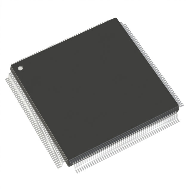
Packaged in a 676-FBGA (27×27) surface-mount case and rated for commercial operation, this device is suited for designs that require a large number of I/Os, moderate embedded memory, and a well-defined supply voltage range for deterministic integration into system boards.
Key Features
- Logic Capacity 38,400 logic elements and 1,500,000 gates provide substantial implementation space for complex combinational and sequential logic.
- Embedded Memory Approximately 0.276 Mbits of on-chip RAM (276,480 bits) to support buffering, state storage, and local data processing without external memory.
- I/O Density 444 user I/Os to support extensive peripheral connectivity and parallel interfaces on a single device.
- Package and Mounting 676-BGA package (supplier device package: 676-FBGA, 27×27) in a surface-mount form factor for compact PCB integration.
- Power Specified supply voltage range of 1.425 V to 1.575 V for predictable power integration and sequencing.
- Operating Range & Grade Commercial grade device rated for operation from 0°C to 85°C.
- RoHS Compliant Designed to meet RoHS environmental requirements for lead-free assembly.
Typical Applications
- I/O‑intensive commercial systems High I/O count (444) enables consolidation of multiple interfaces and peripherals in compact commercial products.
- Embedded logic consolidation 38,400 logic elements and 1,500,000 gates allow integration of control, glue logic, and protocol handling into a single device.
- On‑chip buffering and state storage Approximately 0.276 Mbits of on-chip RAM supports local buffering and state machines without immediate dependence on external memory.
Unique Advantages
- High logic density: 38,400 logic elements and 1.5 million gates let you implement complex logic functions and reduce external ASIC or discrete logic count.
- Substantial I/O resource: 444 user I/Os simplify board-level routing for multi-interface commercial designs, minimizing the need for I/O expansion chips.
- Compact surface-mount packaging: 676-FBGA (27×27) package provides a dense board footprint while maintaining robust pin count for advanced designs.
- Controlled power envelope: Defined supply range of 1.425 V to 1.575 V helps streamline power-supply design and sequencing on the PCB.
- Commercial temperature rating: Specified operation from 0°C to 85°C aligns with standard commercial product requirements.
- RoHS compliance: Supports lead-free assembly and environmental compliance targets.
Why Choose M1A3PE1500-FGG676?
The M1A3PE1500-FGG676 positions itself as a high‑capacity, commercial-grade FPGA option from Microchip Technology that combines extensive logic resources, sizeable on‑chip RAM, and a very large I/O complement in a compact 676-FBGA package. It is a practical choice for engineers and procurement teams designing complex commercial embedded systems that require dense logic integration and broad peripheral connectivity.
For teams focused on reducing BOM complexity and consolidating multiple functions into a single programmable device, this part offers a balance of integration, predictable power requirements, and a standard commercial operating range to support sustained deployment and design scalability.
Request a quote today to check pricing and availability for the M1A3PE1500-FGG676 and to obtain support for your design-in requirements.





















Date Founded: 1989
Headquarters: Chandler, Arizona, USA
Employees: 22,000+
Revenue: $8.349 Billion
Certifications and Memberships: ISO9001:2015, IATF16949:2016, AS 9100D




