
M1AFS1500-1FGG256
| Part Description |
Fusion® Field Programmable Gate Array (FPGA) IC 119 276480 256-LBGA |
|---|---|
| Quantity | 738 Available (as of June 14, 2026) |
| Product Category | Field Programmable Gate Array (FPGA) |
|---|---|
| Manufacturer | Microchip Technology |
| Manufacturing Status | Active |
| Manufacturer Standard Lead Time | 16 Weeks |
| Datasheet |
Specifications & Environmental
| Device Package | 256-FPBGA (17x17) | Grade | Commercial | Operating Temperature | 0°C – 85°C | ||
|---|---|---|---|---|---|---|---|
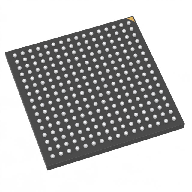
| Package / Case | 256-LBGA | Number of I/O | 119 | Voltage | 1.425 V - 1.575 V | ||
| Mounting Method | Surface Mount | RoHS Compliance | ROHS3 Compliant | REACH Compliance | REACH Unaffected | ||
| Moisture Sensitivity Level | 3 (168 Hours) | Number of LABs/CLBs | 38400 | Number of Logic Elements/Cells | 38400 | ||
| Number of Gates | 1500000 | ECCN | 3A991D | HTS Code | 8542.39.0001 | ||
| Qualification | N/A | Total RAM Bits | 276480 |
Overview of M1AFS1500-1FGG256 – Fusion® Field Programmable Gate Array (FPGA) IC 119 276480 256-LBGA
The M1AFS1500-1FGG256 is a Fusion® Field Programmable Gate Array (FPGA) from Microchip Technology, presented in a 256-LBGA package. It delivers a mid-range programmable logic resource with 38,400 logic elements, approximately 0.276 Mbits of embedded memory, and 119 I/O pins for flexible digital design implementation.
Designed for commercial-grade surface-mount applications, the device supports a core supply range of 1.425 V to 1.575 V and operates between 0 °C and 85 °C. The package and feature set provide a balance of gate density, on-chip memory, and I/O count for integrated digital functions.
Key Features
- Logic Capacity Approximately 38,400 logic elements and 1,500,000 gates to implement medium-complexity programmable logic and custom digital functions.
- Embedded Memory Approximately 0.276 Mbits of on-chip RAM (276,480 bits) for local data storage, buffering, and state retention within logic designs.
- I/O Resources 119 general-purpose I/O pins to support multiple external interfaces, sensor links, and peripheral connections.
- Package Options 256-LBGA package (supplier device package: 256-FPBGA, 17 × 17) suitable for compact surface-mount assemblies.
- Power Core supply voltage range from 1.425 V to 1.575 V to match common FPGA power architectures.
- Operating Range Commercial operating temperature range of 0 °C to 85 °C for standard ambient environments.
- Mounting Surface mount package compatible with modern PCB assembly processes.
- Compliance RoHS compliant, meeting common environmental requirements for electronic assemblies.
Typical Applications
- Commercial Embedded Systems Use the FPGA for programmable logic tasks that require a mix of logic elements, on-chip RAM, and multiple I/O lines within a commercial temperature range.
- Custom Interface and Glue Logic Implement protocol bridging, custom I/O routing, and timing-critical interfacing using the 119 available I/O pins and programmable logic fabric.
- Prototyping and Design Iteration Leverage the reprogrammable logic capacity and on-chip memory for rapid prototyping of medium-complexity digital functions and system validation.
Unique Advantages
- Balanced Logic Density: 38,400 logic elements and 1,500,000 gates provide a mid-range capacity that balances integration and cost for many commercial designs.
- On-Chip Memory: Approximately 0.276 Mbits of embedded RAM reduces external memory needs for buffering and state machines, simplifying BOM and board layout.
- Generous I/O Count: 119 I/O pins enable multiple peripheral and interface connections without immediate need for external I/O expanders.
- Compact Package: 256-LBGA (17 × 17 FPBGA) offers a compact footprint for space-constrained PCBs while maintaining robust pin count.
- Commercial Temperature and RoHS Compliance: 0 °C to 85 °C operating range and RoHS compliance make the device suitable for standard commercial product deployments.
- Defined Power Range: Specified core supply between 1.425 V and 1.575 V enables predictable power design and regulation selection.
Why Choose M1AFS1500-1FGG256?
The M1AFS1500-1FGG256 combines a mid-range logic fabric with on-chip memory and a substantial I/O complement in a compact 256-LBGA package. Its mix of 38,400 logic elements, approximately 0.276 Mbits of embedded RAM, and 119 I/O make it well suited to commercial embedded designs that require flexible, reconfigurable digital resources without moving to higher-density FPGA families.
With defined power and thermal ranges and RoHS compliance, this Fusion® FPGA is a practical choice for designers seeking a programmable logic device that integrates moderate logic, memory, and interface capacity into a surface-mount package from Microchip Technology.
Request a quote or submit an inquiry to receive pricing and availability for the M1AFS1500-1FGG256. Include your quantity and lead-time requirements to get a tailored response.


Date Founded: 1989
Headquarters: Chandler, Arizona, USA
Employees: 22,000+
Revenue: $8.349 Billion
Certifications and Memberships: ISO9001:2015, IATF16949:2016, AS 9100D


