
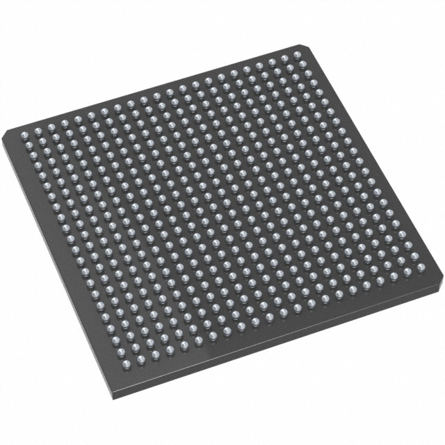
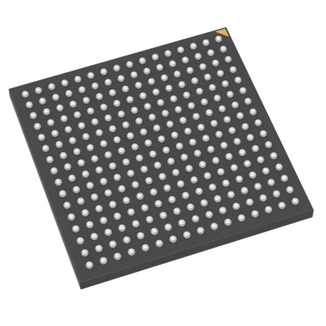
M1AFS600-2FGG484
| Part Description |
Fusion® Field Programmable Gate Array (FPGA) IC 172 110592 484-BGA |
|---|---|
| Quantity | 912 Available (as of June 18, 2026) |

| Product Category | Field Programmable Gate Array (FPGA) |
|---|---|
| Manufacturer | Microchip Technology |
| Manufacturing Status | Active |
| Manufacturer Standard Lead Time | 16 Weeks |
| Datasheet |
Specifications & Environmental
| Device Package | 484-FPBGA (23x23) | Grade | Commercial | Operating Temperature | 0°C – 85°C | ||
|---|---|---|---|---|---|---|---|
| Package / Case | 484-BGA | Number of I/O | 172 | Voltage | 1.425 V - 1.575 V | ||
| Mounting Method | Surface Mount | RoHS Compliance | ROHS3 Compliant | REACH Compliance | REACH Unaffected | ||
| Moisture Sensitivity Level | 3 (168 Hours) | Number of LABs/CLBs | 13824 | Number of Logic Elements/Cells | 13824 | ||
| Number of Gates | 600000 | ECCN | 3A991D | HTS Code | 8542.39.0001 | ||
| Qualification | N/A | Total RAM Bits | 110592 |
Overview of M1AFS600-2FGG484 – Fusion® Field Programmable Gate Array (FPGA) IC 172 110592 484-BGA
The M1AFS600-2FGG484 is a Fusion® Field Programmable Gate Array (FPGA) from Microchip Technology, provided in a 484-BGA (23×23) package. It delivers a mid-range programmable logic resource set intended for designers who need a compact, surface-mount FPGA with substantial I/O and on-chip memory.
With 13,824 logic elements, approximately 0.11 Mbits of embedded RAM, and 172 I/O pins, this commercial-grade device is suited to a variety of digital-logic implementations where board-level integration, density, and power-supply compatibility are key considerations.
Key Features
- Logic Capacity 13,824 logic elements (cells) and an effective gate count of 600,000 provide the programmable fabric for implementing complex combinational and sequential logic.
- Embedded Memory Approximately 0.11 Mbits of on-chip RAM (110,592 bits) for buffering, FIFOs, or small data structures used by implemented functions.
- I/O Density 172 user I/O pins enable broad interfacing options for peripherals, buses, and external devices.
- Power Supply Core voltage range of 1.425 V to 1.575 V to match target board-level power architectures.
- Package & Mounting 484-ball FPBGA (23×23) package in a surface-mount form factor, suitable for compact, high-I/O designs.
- Operating Range & Grade Commercial-grade device specified for operation from 0 °C to 85 °C.
- Compliance RoHS-compliant construction for regulatory and assembly considerations.
Typical Applications
- Custom digital logic Implement glue logic, protocol converters, and application-specific processing using the device’s 13,824 logic elements and flexible I/O.
- Interface bridging Use the 172 I/O pins to bridge multiple peripherals or bus standards on a single board-level FPGA.
- Prototyping and development Leverage the device’s mid-range logic and embedded RAM for validating designs and building proof-of-concept systems.
Unique Advantages
- Balanced logic and memory: 13,824 logic elements combined with approximately 0.11 Mbits of RAM support moderately complex logic and small on-chip data storage without external memory.
- High I/O count in a compact package: 172 I/O pins in a 484-BGA (23×23) surface-mount package allow dense interfacing while minimizing board area.
- Clear power requirements: A defined core voltage range (1.425 V–1.575 V) simplifies power-supply design and board integration.
- Commercial operating range: Specified operation from 0 °C to 85 °C for typical commercial applications.
- Regulatory readiness: RoHS compliance supports environmentally conscious product assembly and manufacturing.
- Manufacturer backing: Produced by Microchip Technology, offering continuity for sourcing and documentation.
Why Choose M1AFS600-2FGG484?
The M1AFS600-2FGG484 is positioned for designers needing a mid-density FPGA with a strong mix of logic elements, embedded RAM, and a high I/O count in a compact 484-BGA surface-mount package. Its specified core voltage range and commercial operating temperature make it straightforward to integrate into standard embedded designs.
Choose this device when your design requires the flexibility of programmable logic combined with on-chip memory and plentiful I/O, backed by Microchip Technology documentation and product availability for production and prototyping projects.
Request a quote or submit a pricing and availability inquiry to evaluate M1AFS600-2FGG484 for your next design.


Date Founded: 1989
Headquarters: Chandler, Arizona, USA
Employees: 22,000+
Revenue: $8.349 Billion
Certifications and Memberships: ISO9001:2015, IATF16949:2016, AS 9100D


