
M2GL150-1FCS536
| Part Description |
IGLOO2 Field Programmable Gate Array (FPGA) IC 293 5120000 146124 536-LFBGA, CSPBGA |
|---|---|
| Quantity | 1,331 Available (as of October 7, 2026) |

| Product Category | Field Programmable Gate Array (FPGA) |
|---|---|
| Manufacturer | Microchip Technology |
| Manufacturing Status | Active |
| Manufacturer Standard Lead Time | 10 Weeks |
| Datasheet |
Specifications & Environmental
| Device Package | 536-CSPBGA (16x16) | Grade | Commercial | Operating Temperature | 0°C – 85°C | ||
|---|---|---|---|---|---|---|---|
| Package / Case | 536-LFBGA, CSPBGA | Number of I/O | 293 | Voltage | 1.14 V - 2.625 V | ||
| Mounting Method | Surface Mount | RoHS Compliance | RoHS non-compliant | REACH Compliance | REACH Unaffected | ||
| Moisture Sensitivity Level | 3 (168 Hours) | Number of LABs/CLBs | 146124 | Number of Logic Elements/Cells | 146124 | ||
| Number of Gates | N/A | ECCN | 3A991B2 | HTS Code | 8542.39.0001 | ||
| Qualification | N/A | Total RAM Bits | 5120000 |
Overview of M2GL150-1FCS536 – IGLOO2 Field Programmable Gate Array (FPGA), 536-LFBGA
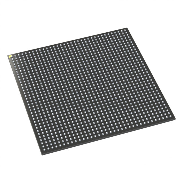
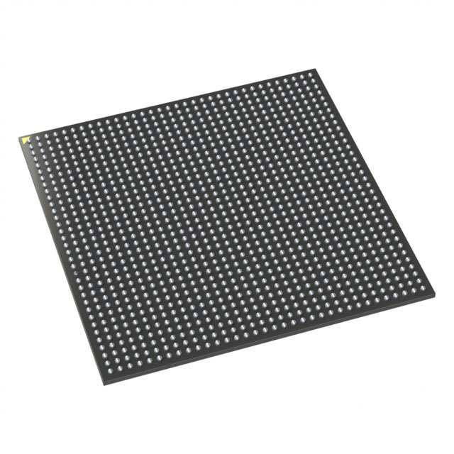
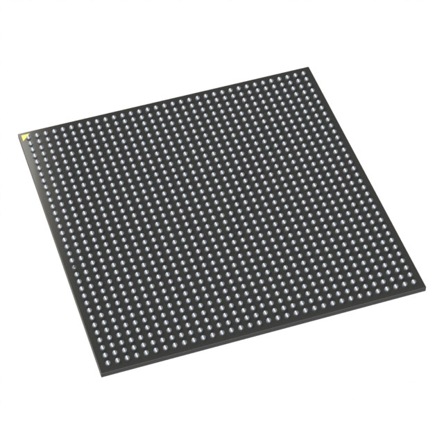
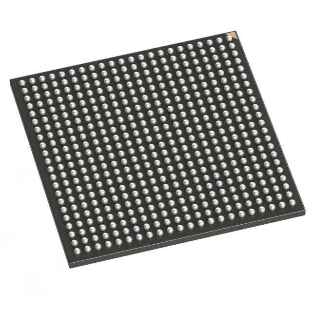
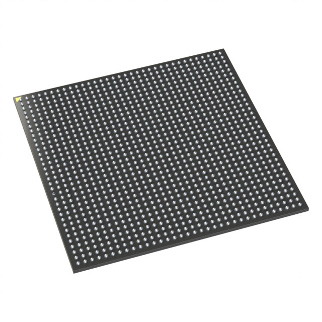
The M2GL150-1FCS536 is an IGLOO2 family FPGA IC from Microchip Technology configured in a 536-LFBGA (536-CSPBGA, 16×16) surface-mount package. It provides 146,124 logic elements and approximately 5.12 Mbits of embedded RAM, along with 293 user I/Os for complex digital interfacing.
Designed for commercial-grade embedded designs, the device operates from a supply voltage range of 1.14 V to 2.625 V and across an operating temperature range of 0 °C to 85 °C. It is RoHS compliant and intended for applications that require substantial on-chip logic and memory capacity in a compact BGA footprint.
Key Features
- Logic Capacity — 146,124 logic elements suitable for large-scale combinational and sequential logic implementations.
- Embedded Memory — Total on-chip RAM of 5,120,000 bits (approximately 5.12 Mbits) to support buffering, state storage, and data processing functions.
- I/O Density — 293 user I/Os to support multiple interfaces, peripherals, and high-pin-count connectivity.
- Power — Flexible supply voltage range from 1.14 V to 2.625 V to accommodate diverse core and I/O voltage requirements.
- Package and Mounting — 536-LFBGA (536-CSPBGA, 16×16) surface-mount package offering a compact footprint for space-constrained boards.
- Operating Range — Commercial grade with an operating temperature range of 0 °C to 85 °C.
- Compliance — RoHS compliant for environmental and regulatory alignment.
Typical Applications
- Commercial Embedded Systems — Suitable for embedded designs that require substantial logic and on-chip memory in a commercial-grade device.
- High-Density I/O Interfaces — Use where large numbers of signals and peripherals must be routed and managed from a single FPGA.
- Custom Digital Processing — Implement custom data paths, control logic, and state machines using the available logic elements and embedded RAM.
Unique Advantages
- High Logic Integration: 146,124 logic elements consolidate complex digital functions into a single device, reducing component count.
- Substantial On-Chip Memory: Approximately 5.12 Mbits of embedded RAM supports buffering and local data storage without external memory.
- Large I/O Count: 293 I/Os enable flexible connectivity to multiple peripherals and interfaces from one FPGA.
- Compact BGA Package: The 536-LFBGA (16×16) CSPBGA package provides a dense, space-saving solution for compact boards.
- Broad Voltage Support: Operates across 1.14 V to 2.625 V, accommodating a range of core and I/O voltage domains.
- Regulatory Compliance: RoHS compliance supports environmentally conscious designs and manufacturing.
Why Choose M2GL150-1FCS536?
The M2GL150-1FCS536 balances high logic capacity, significant embedded memory, and extensive I/O in a compact 536-LFBGA surface-mount package, making it a practical choice for commercial embedded designs that demand integration and board-space efficiency. Its supply voltage flexibility and RoHS compliance further support diverse design requirements within the specified commercial temperature range.
This device is well suited to designers and teams building systems that require consolidation of digital functions, on-chip data storage, and high pin-count interfacing while maintaining a commercial-grade specification and compact form factor.
Request a quote or submit a sales inquiry to check availability and pricing for the M2GL150-1FCS536.




















Date Founded: 1989
Headquarters: Chandler, Arizona, USA
Employees: 22,000+
Revenue: $8.349 Billion
Certifications and Memberships: ISO9001:2015, IATF16949:2016, AS 9100D




