
M7AFS600-FGG256I
| Part Description |
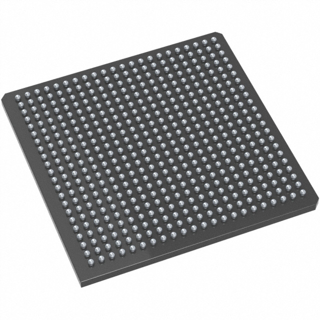
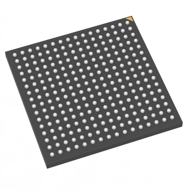
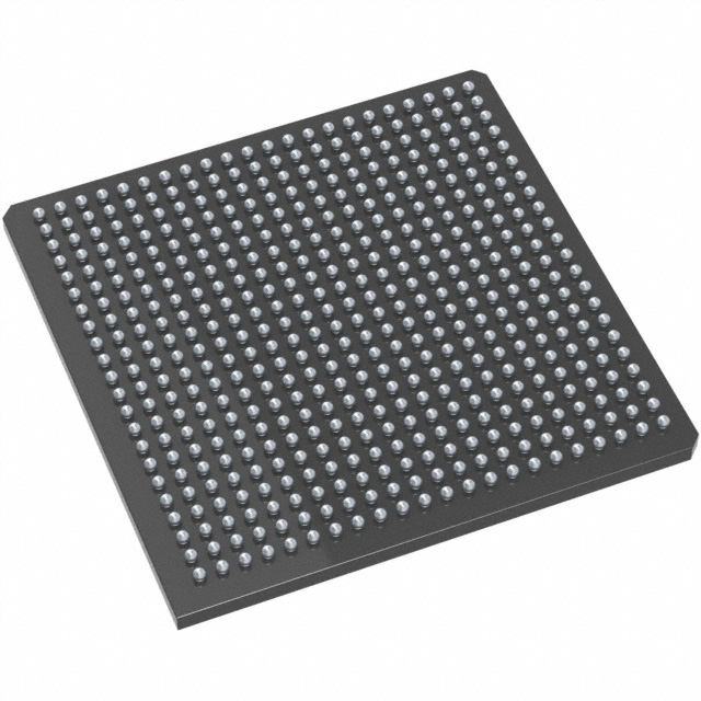
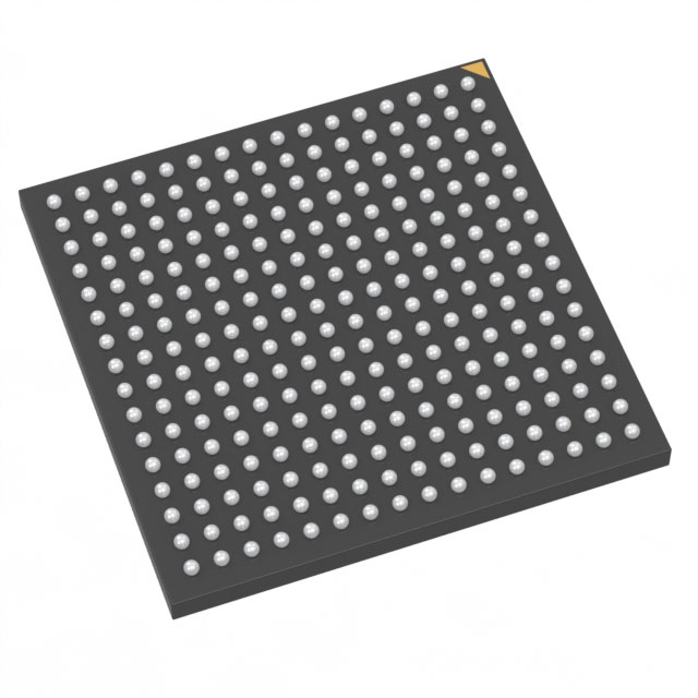
Fusion® Field Programmable Gate Array (FPGA) IC 119 110592 256-LBGA |
|---|---|
| Quantity | 1,355 Available (as of October 8, 2026) |

| Product Category | Field Programmable Gate Array (FPGA) |
|---|---|
| Manufacturer | Microchip Technology |
| Manufacturing Status | Active |
| Manufacturer Standard Lead Time | 16 Weeks |
| Datasheet |
Specifications & Environmental
| Device Package | 256-FPBGA (17x17) | Grade | Industrial | Operating Temperature | -40°C – 85°C | ||
|---|---|---|---|---|---|---|---|
| Package / Case | 256-LBGA | Number of I/O | 119 | Voltage | 1.425 V - 1.575 V | ||
| Mounting Method | Surface Mount | RoHS Compliance | ROHS3 Compliant | REACH Compliance | REACH Unaffected | ||
| Moisture Sensitivity Level | 3 (168 Hours) | Number of LABs/CLBs | 13824 | Number of Logic Elements/Cells | 13824 | ||
| Number of Gates | 600000 | ECCN | 3A991D | HTS Code | 8542.39.0001 | ||
| Qualification | N/A | Total RAM Bits | 110592 |
Overview of M7AFS600-FGG256I – Fusion® Field Programmable Gate Array (FPGA) IC 119 110592 256-LBGA
The M7AFS600-FGG256I is a Fusion® family mixed-signal FPGA featuring flash-based, nonvolatile configuration and an array of integrated analog and digital resources. Built for industrial applications, this surface-mount device combines approximately 13,824 logic elements, roughly 108 kbits (110,592 bits) of embedded RAM, and 600,000 system gates to enable reprogrammable, compact system designs.
Optimized for mixed-signal control, data acquisition and embedded logic tasks, the device delivers fast system responsiveness, on-chip analog resources and secure in-system programmability to simplify designs that require both digital and analog integration.
Key Features
- Flash-Based Nonvolatile Architecture Advanced flash-based CMOS process provides reprogrammable, instant-on operation and retains configuration when powered off.
- Logic Capacity Approximately 13,824 logic elements and 600,000 system gates for mid-range FPGA designs.
- Embedded Memory Approximately 108 kbits (110,592 bits) of embedded RAM and 4 Mbits of on-chip flash memory (two 2-Mbit blocks) for code, data buffering and state retention.
- Analog and A/D Capabilities Integrated analog resources include up to 30 analog input channels and an ADC supporting up to 12-bit resolution and up to 600 ksps sampling rates, with internal or external reference options.
- On-Chip Clocking and PLLs Multiple clock conditioning circuits with up to two integrated PLLs enable flexible frequency synthesis and clock distribution for system-level timing.
- Advanced Digital I/O 119 I/Os in the 256-LBGA package with support for bank-selectable I/O voltages (1.5 V, 1.8 V, 2.5 V, 3.3 V), single-ended and differential standards, programmable drive strength and slew rates.
- Power and Low-Power Modes Core supply tolerance 1.425 V to 1.575 V; device operation supported by a single 3.3 V supply with an on-chip 1.5 V regulator and low-power sleep/standby modes.
- In-System Programming and Security ISP via JTAG with 128-bit AES and FlashLock® support for secure remote programming and protection of FPGA contents.
- Package and Temperature Grade 256-LBGA (256-FPBGA, 17×17) surface-mount package rated for industrial temperature operation from −40 °C to 85 °C and RoHS compliant.
Typical Applications
- Industrial Control and Automation Mixed-signal I/Os and MOSFET gate-driver capability make the device suitable for motor control, power conversion supervisory functions and embedded control loops.
- Sensor Acquisition and Conditioning On-chip ADC channels and internal monitoring blocks enable direct interfacing to analog sensors for measurement, filtering and preprocessing.
- Embedded Logic and Glue Mid-range logic capacity and flexible I/O voltages provide programmable glue logic, protocol adaptation and interface bridging in compact systems.
- Board Management and System Supervision Nonvolatile flash and secure ISP support firmware updates, watchdog-style logic and system management roles in remote or distributed equipment.
Unique Advantages
- Nonvolatile, Instant-On Operation: Flash-based configuration eliminates external configuration memory and delivers immediate startup with retained programming across power cycles.
- Tightly Integrated Mixed-Signal Resources: Embedded ADCs, analog inputs and gate-driver outputs reduce external component count and simplify sensor and power-control implementations.
- Secure In-System Programming: 128-bit AES ISP and FlashLock® support secure updates and help protect intellectual property on deployed units.
- Flexible I/O and Clocking: Bank-selectable voltage support, differential standards and multiple clock conditioning circuits with PLLs enable easy interfacing and precise timing control.
- Industrial Temperature and RoHS Compliance: Designed for −40 °C to 85 °C operation and RoHS-compliant manufacturing for industrial deployments.
Why Choose M7AFS600-FGG256I?
The M7AFS600-FGG256I positions itself as a versatile mid-range Fusion® FPGA that brings together nonvolatile flash configuration, substantial logic density and on-chip analog capabilities in a single 256-LBGA package. Its combination of approximately 13,824 logic elements, embedded RAM and multiple ADC channels addresses designs that require integrated mixed-signal processing without a large external BOM.
This device is well suited to engineers building industrial control, data acquisition and embedded management systems who need secure in-field programmability, flexible I/O voltage support and reliable operation across industrial temperature ranges. The Fusion® family feature set supports scalable designs and long-term maintainability via secure ISP and on-chip flash.
Request a quote or submit a pricing inquiry to get availability and lead-time information for M7AFS600-FGG256I.
























Date Founded: 1989
Headquarters: Chandler, Arizona, USA
Employees: 22,000+
Revenue: $8.349 Billion
Certifications and Memberships: ISO9001:2015, IATF16949:2016, AS 9100D




