
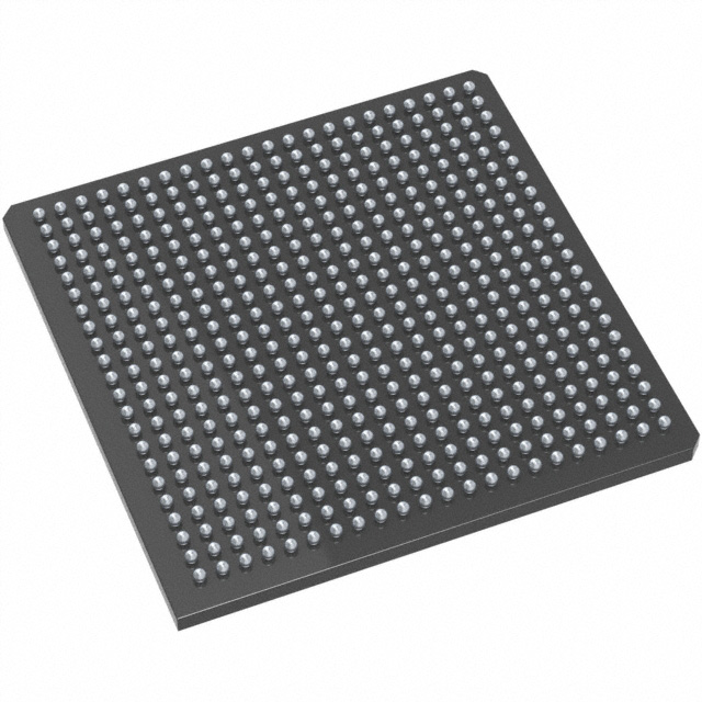
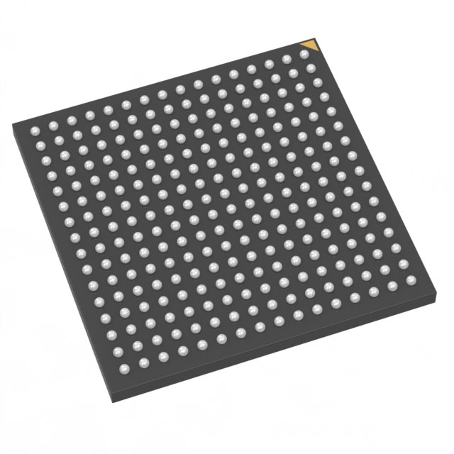
M7AFS600-FG484
| Part Description |
Fusion® Field Programmable Gate Array (FPGA) IC 172 110592 484-BGA |
|---|---|
| Quantity | 1,958 Available (as of June 18, 2026) |

| Product Category | Field Programmable Gate Array (FPGA) |
|---|---|
| Manufacturer | Microchip Technology |
| Manufacturing Status | Active |
| Manufacturer Standard Lead Time | 16 Weeks |
| Datasheet |
Specifications & Environmental
| Device Package | 484-FPBGA (23x23) | Grade | Commercial | Operating Temperature | 0°C – 70°C | ||
|---|---|---|---|---|---|---|---|
| Package / Case | 484-BGA | Number of I/O | 172 | Voltage | 1.425 V - 1.575 V | ||
| Mounting Method | Surface Mount | RoHS Compliance | RoHS non-compliant | REACH Compliance | REACH Unaffected | ||
| Moisture Sensitivity Level | 3 (168 Hours) | Number of LABs/CLBs | 13824 | Number of Logic Elements/Cells | 13824 | ||
| Number of Gates | 600000 | ECCN | 3A991D | HTS Code | 8542.39.0001 | ||
| Qualification | N/A | Total RAM Bits | 110592 |
Overview of M7AFS600-FG484 – Fusion® Field Programmable Gate Array (FPGA) IC 172 110592 484-BGA
The M7AFS600-FG484 is a Fusion® family mixed-signal, flash-based FPGA from Microchip Technology. It pairs nonvolatile on-chip flash configuration with integrated analog resources and high-density digital fabric to address mixed-signal control, board-management, and mezzanine applications.
Built around approximately 600,000 system gates and 13,824 logic elements, this commercial-grade device provides high I/O count and embedded memory along with integrated ADCs, MOSFET gate drivers and clocking resources for compact, single-chip system designs.
Key Features
- Logic and Capacity — 13,824 logic elements (tiles) and approximately 600,000 system gates provide substantial programmable logic density for control and interface functions.
- Embedded Memory — Approximately 4 Mbits of embedded flash for configuration and user code plus approximately 0.11 Mbits (110,592 bits) of on-chip RAM for data buffering and state storage.
- Mixed-Signal Integration — Integrated A/D converters up to 12-bit resolution and up to 600 ksps, with up to 30 analog input channels and internal/external reference options; current and temperature monitoring blocks.
- MOSFET Gate Drivers — Up to 10 gate-driver outputs with P- and N‑channel MOSFET support and programmable drive strengths (including microamp and 20 mA ranges) for direct power-stage interfacing.
- On-Chip Clocking and PLLs — Internal 100 MHz RC oscillator (±1% accuracy), crystal oscillator support (32 kHz–20 MHz), six Clock Conditioning Circuits with integrated PLLs (AFS600 includes two PLLs) for flexible frequency management.
- Advanced I/O — Up to 172 digital I/Os, bank-selectable mixed-voltage operation (1.5 V, 1.8 V, 2.5 V, 3.3 V), support for single-ended and differential standards, programmable slew/drive and hot-swap capable I/Os.
- Security and In-System Programming — In-System Programming (ISP) with 128-bit AES and FlashLock® support to protect FPGA contents and enable secure updates via JTAG.
- Power and Low-Power Modes — Single 3.3 V primary supply with on-chip 1.5 V regulator; sleep and standby modes to help manage system power.
- Package and Temperature — 484-ball FPBGA (23 × 23) surface-mount package; commercial operating temperature range 0 °C to 70 °C.
- Compliance — RoHS compliant.
Typical Applications
- ATCA and Board Management — Targeted Pigeon Point ATCA IP support and Board Management Reference (BMR) starter kit compatibility for system management implementations.
- Advanced Mezzanine and Module Designs — MicroBlade Advanced Mezzanine Card support (AdvancedMC™ designs) for mezzanine modules and carrier boards.
- Mixed-Signal Sensor Acquisition — On-chip ADCs and analog I/O enable direct sensor signal acquisition and front-end integration without extensive external components.
- Power-Stage and MOSFET Control — Integrated gate drivers and high-voltage-tolerant analog inputs allow direct interfacing to MOSFETs and power-management circuits.
Unique Advantages
- Nonvolatile, Instant-On Capability: Flash-based configuration retains program state when powered off and enables immediate startup without external configuration memories.
- Highly Integrated Mixed-Signal Peripherals: ADCs, analog inputs, and MOSFET gate drivers reduce external BOM and simplify mixed-signal system designs.
- Flexible I/O Voltage Support: Bank-selectable I/O voltages and broad I/O standard support simplify board-level interfacing across multiple voltage domains.
- Secure In-System Updates: 128-bit AES ISP and FlashLock® support help protect intellectual property and enable secure field updates.
- Scalable Fusion Family Compatibility: Pin-compatible packages across the Fusion family provide migration and scaling options within the same package footprint.
- Compact, High-I/O Package: 484-FPBGA (23×23) delivers up to 172 digital I/Os in a surface-mount BGA suitable for space-constrained boards.
Why Choose M7AFS600-FG484?
The M7AFS600-FG484 combines flash-based nonvolatile configuration, significant programmable logic capacity, and integrated mixed-signal peripherals to deliver a compact, single-chip solution for board management, mezzanine modules, and mixed-signal control applications. Its combination of embedded flash, on-chip RAM, ADCs, gate drivers and flexible I/O makes it well suited for designs that require integration of analog and digital functions while minimizing external components.
As a commercial-grade device within the Fusion® family, it offers a scalable path for designs that need secure in-system programming, configurable clocking with PLLs, and robust I/O options—enabling designers to consolidate functionality and simplify system architecture.
Request a quote or submit an inquiry to receive pricing and availability information for the M7AFS600-FG484.


Date Founded: 1989
Headquarters: Chandler, Arizona, USA
Employees: 22,000+
Revenue: $8.349 Billion
Certifications and Memberships: ISO9001:2015, IATF16949:2016, AS 9100D


