
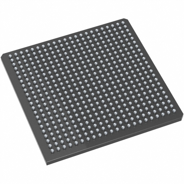
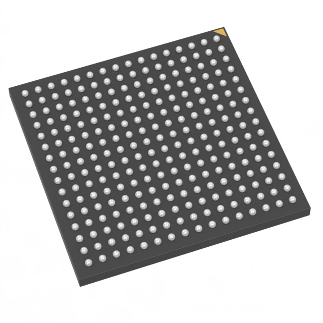
M7AFS600-FG256
| Part Description |
Fusion® Field Programmable Gate Array (FPGA) IC 119 110592 256-LBGA |
|---|---|
| Quantity | 968 Available (as of June 16, 2026) |

| Product Category | Field Programmable Gate Array (FPGA) |
|---|---|
| Manufacturer | Microchip Technology |
| Manufacturing Status | Active |
| Manufacturer Standard Lead Time | 16 Weeks |
| Datasheet |
Specifications & Environmental
| Device Package | 256-FPBGA (17x17) | Grade | Commercial | Operating Temperature | 0°C – 70°C | ||
|---|---|---|---|---|---|---|---|
| Package / Case | 256-LBGA | Number of I/O | 119 | Voltage | 1.425 V - 1.575 V | ||
| Mounting Method | Surface Mount | RoHS Compliance | RoHS non-compliant | REACH Compliance | REACH Unaffected | ||
| Moisture Sensitivity Level | 3 (168 Hours) | Number of LABs/CLBs | 13824 | Number of Logic Elements/Cells | 13824 | ||
| Number of Gates | 600000 | ECCN | 3A991D | HTS Code | 8542.39.0001 | ||
| Qualification | N/A | Total RAM Bits | 110592 |
Overview of M7AFS600-FG256 – Fusion® Field Programmable Gate Array (FPGA) IC 119 110592 256-LBGA
The M7AFS600-FG256 is a Fusion family mixed-signal Flash-based FPGA that combines nonvolatile reprogrammable logic with integrated analog and system peripherals. It provides 600,000 system gates, 13,824 logic elements, and mixed-signal resources targeted at designs that require on-chip flash configuration, analog data acquisition and programmable I/O.
This device is suited to commercial embedded and control applications that benefit from integrated ADC channels, MOSFET gate drivers, on-chip clocking and security features, while offering a 256-LBGA surface-mount package and commercial temperature grading.
Key Features
- Logic Capacity — 600,000 system gates and 13,824 logic elements, providing a substantial programmable fabric for complex logic and control functions.
- On-Chip Memory — Approximately 110,592 bits (≈108 kbits) of embedded RAM across multiple SRAM blocks for FIFOs and data buffering.
- Embedded Flash Configuration — Fusion family flash-based reprogrammable technology with nonvolatile configuration and instant-on behavior; AFS600 family devices include 4 Mbits of on-chip Flash memory.
- Analog Integration — Integrated ADC capability up to 12-bit resolution and up to 600 ksps with up to 30 analog input channels; includes current and temperature monitor blocks and high-voltage input tolerance.
- MOSFET Gate Drivers — Up to 10 MOSFET gate driver outputs with programmable drive strengths and support for P- and N-channel power MOSFETs.
- Clocking and PLLs — Internal 100 MHz RC oscillator (accurate to 1%), crystal oscillator support (32 kHz–20 MHz), multiple clock conditioning circuits and integrated PLLs (AFS600 includes 2 PLLs) enabling up to 350 MHz system performance.
- Advanced I/O — 119 I/O pins (package-dependent), bank-selectable mixed-voltage I/O (1.5 V, 1.8 V, 2.5 V, 3.3 V), differential and single-ended standards, and support for high-speed DDR operation up to 700 Mbps.
- Security and In-System Programming — ISP support with 128-bit AES via JTAG and FlashLock for protecting FPGA contents.
- Power and Packaging — Voltage supply range 1.425 V to 1.575 V; single-chip surface mount 256-LBGA package (supplier device package: 256-FPBGA, 17×17); commercial operating temperature 0 °C to 70 °C; RoHS compliant.
Typical Applications
- Mixed-signal control and monitoring — Use integrated ADC channels and analog I/O for sensor interfacing, system monitoring and mixed-signal processing in embedded controllers.
- Power conversion and motor control — On-chip MOSFET gate drivers, high-voltage input tolerance and programmable drive strengths support power-stage control and motor-drive applications.
- High-speed digital interfaces — Differential I/O standards and DDR-capable I/O enable high-throughput communication links and protocol bridging.
- Secure, reprogrammable systems — Flash-based nonvolatile configuration and AES-protected ISP allow secure field updates and in-system reconfiguration.
Unique Advantages
- Flash-based nonvolatile configuration: Retains program when powered off and supports instant-on single-chip operation, reducing external configuration components.
- Integrated mixed-signal peripherals: ADC channels, analog monitoring and MOSFET gate drivers reduce BOM and simplify board-level design for analog‑aware applications.
- Flexible I/O options: Bank-selectable mixed-voltage I/O and support for multiple differential and single-ended standards enable easy interfacing with a wide range of peripherals and transceivers.
- Built-in security and ISP: 128-bit AES via JTAG and FlashLock help protect IP and support secure in-field updates.
- Compact commercial package: 256-LBGA (256-FPBGA 17×17) surface-mount package provides a balance of I/O count (119) and board-space efficiency for compact designs.
Why Choose M7AFS600-FG256?
The M7AFS600-FG256 brings Fusion family mixed-signal integration to designs that need substantial programmable logic (600,000 gates, 13,824 logic elements) together with embedded memory and analog resources. Its flash-based nonvolatile configuration, secure ISP and on-chip peripherals make it a practical choice for commercial embedded systems that require reprogrammability, analog interfacing and robust I/O flexibility.
This device is well suited for engineers developing control, monitoring and high-speed interface applications who value on-chip analog functionality, MOSFET drive capability and secure in-system updates within a 256-LBGA surface-mount footprint.
Request a quote or submit a pricing and availability inquiry to evaluate the M7AFS600-FG256 for your next mixed-signal FPGA design.


Date Founded: 1989
Headquarters: Chandler, Arizona, USA
Employees: 22,000+
Revenue: $8.349 Billion
Certifications and Memberships: ISO9001:2015, IATF16949:2016, AS 9100D


