
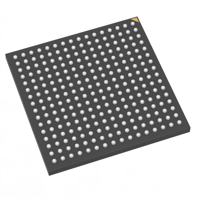
M7AFS600-FG256I
| Part Description |
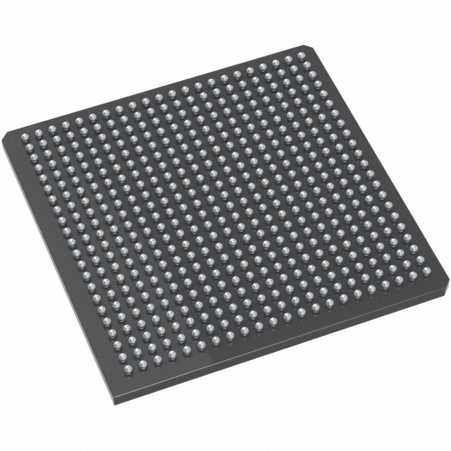
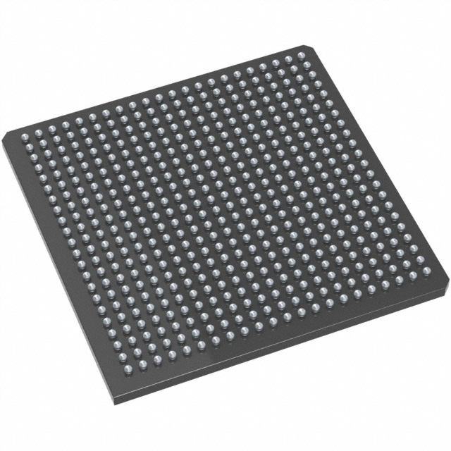
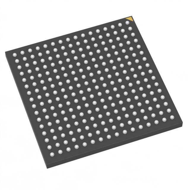
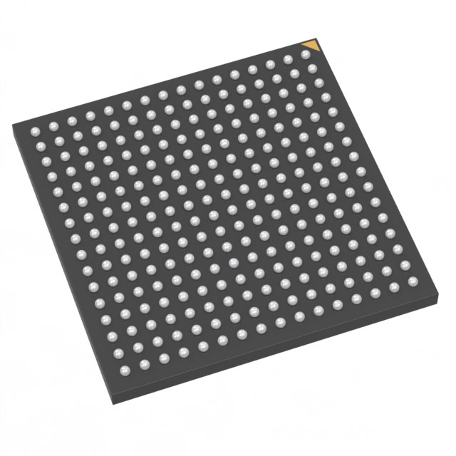
Fusion® Field Programmable Gate Array (FPGA) IC 119 110592 256-LBGA |
|---|---|
| Quantity | 50 Available (as of October 8, 2026) |
| Product Category | Field Programmable Gate Array (FPGA) |
|---|---|
| Manufacturer | Microchip Technology |
| Manufacturing Status | Active |
| Manufacturer Standard Lead Time | 16 Weeks |
| Datasheet |
Specifications & Environmental
| Device Package | 256-FPBGA (17x17) | Grade | Industrial | Operating Temperature | -40°C – 85°C | ||
|---|---|---|---|---|---|---|---|
| Package / Case | 256-LBGA | Number of I/O | 119 | Voltage | 1.425 V - 1.575 V | ||
| Mounting Method | Surface Mount | RoHS Compliance | RoHS non-compliant | REACH Compliance | REACH Unaffected | ||
| Moisture Sensitivity Level | 3 (168 Hours) | Number of LABs/CLBs | 13824 | Number of Logic Elements/Cells | 13824 | ||
| Number of Gates | 600000 | ECCN | 3A991D | HTS Code | 8542.39.0001 | ||
| Qualification | N/A | Total RAM Bits | 110592 |
Overview of M7AFS600-FG256I – Fusion® Field Programmable Gate Array (FPGA) IC 119 110592 256-LBGA
The M7AFS600-FG256I is a Fusion family mixed-signal, flash-based FPGA offering 600,000 system gates and 13,824 logic elements for complex logic implementations. Built for embedded and industrial applications, it combines programmable logic, embedded memory and integrated analog peripherals to enable system integration, secure in-system programming and rapid start-up behavior.
Key platform attributes include approximately 110,592 bits of embedded RAM, family-level 4 Mbits of flash configuration memory, up to 119 general-purpose I/Os in a bank-selectable mixed-voltage architecture, and industrial-grade operation from −40 °C to +85 °C in a 256-LBGA surface-mount package.
Key Features
- Core — 600,000 system gates and 13,824 logic elements (tiles) provide substantial programmable logic capacity; Fusion family performance up to 350 MHz supports demanding control and data-path designs.
- Embedded Memory — Approximately 110,592 bits (≈108 kbits) of on-chip RAM for buffering and temporary data storage; Fusion AFS600 devices include 4 Mbits of flash configuration memory.
- Mixed-Signal Integration — Integrated ADCs with up to 12-bit resolution and up to 600 ksps, supporting up to 30 analog input channels and dedicated MOSFET gate-driver outputs (up to 10) for power-stage control.
- Advanced I/O — 119 I/O pins with bank-selectable voltages (1.5 V, 1.8 V, 2.5 V, 3.3 V) and support for single-ended and differential standards including LVTTL, LVCMOS, LVPECL and LVDS.
- Clocking and Timing — Internal 100 MHz RC oscillator, multiple clock-conditioning circuits and two PLLs (AFS600 family) for flexible clock generation and distribution.
- Power and Packaging — Surface-mount 256-LBGA (256-FPBGA, 17×17) package; core voltage supply 1.425–1.575 V; family supports single 3.3 V supply with on-chip 1.5 V regulator.
- Security and ISP — In-system programming (ISP) with 128-bit AES via JTAG and FlashLock® protection mechanisms for secure configuration and updates.
- Industrial Grade Operation — Rated for −40 °C to +85 °C operating temperature and specified as industrial grade for deployment in temperature-variable environments.
Typical Applications
- Industrial Control and Automation — Combine on-chip ADCs, logic and gate drivers for motor control, power management and factory automation functions operating across industrial temperature ranges.
- Power Conversion and Motor Drives — Dedicated MOSFET gate-driver outputs and accurate ADC channels enable on-device control of power stages and gate-drive systems.
- Sensor and Data-Acquisition Systems — Multiple analog input channels and embedded RAM support local signal conditioning, buffering and acquisition for monitoring applications.
- High-Speed Digital Interfaces — Mixed single-ended and differential I/O support facilitates implementation of high-speed serial or parallel interfaces and domain bridging.
Unique Advantages
- Highly integrated mixed-signal solution: Programmable logic, ADCs, gate drivers and embedded flash reduce external components and simplify board-level design.
- Nonvolatile, instant-on configuration: Flash-based configuration memory retains programming without external configuration devices and enables rapid start-up.
- Flexible I/O voltage support: Bank-selectable 1.5 V–3.3 V I/O eases interfacing with a wide range of peripherals and logic families.
- Robust on-chip timing: Internal oscillator, CCCs and two PLLs provide flexible clocking without extensive external timing components.
- Engineered for industrial use: Industrial temperature rating and surface-mount 256-LBGA packaging support reliable deployment in harsh environments.
Why Choose M7AFS600-FG256I?
The M7AFS600-FG256I positions itself as a versatile mixed-signal FPGA that balances substantial programmable logic resources with integrated analog peripherals and nonvolatile flash configuration. Its combination of 600k gates, 13,824 logic elements, embedded RAM and ADC/gate-driver capability makes it suitable for embedded industrial designs that require tight integration between control logic and analog/power subsystems.
Designers targeting industrial control, power conversion, sensor acquisition and mixed-signal interface applications will benefit from the M7AFS600-FG256I’s secure in-system programming, flexible I/O voltages, and industrial temperature rating, delivering a compact platform for long-term, scalable product designs.
Request a quote or submit an inquiry to obtain pricing and availability for the M7AFS600-FG256I.






















Date Founded: 1989
Headquarters: Chandler, Arizona, USA
Employees: 22,000+
Revenue: $8.349 Billion
Certifications and Memberships: ISO9001:2015, IATF16949:2016, AS 9100D




