
ORT8850L-1BMN680C
| Part Description |
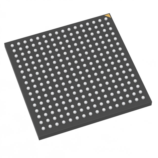
ORCA® 4 Field Programmable Gate Array (FPGA) IC 278 75776 4992 680-BBGA |
|---|---|
| Quantity | 370 Available (as of October 7, 2026) |

| Product Category | Field Programmable Gate Array (FPGA) |
|---|---|
| Manufacturer | Lattice Semiconductor Corporation |
| Manufacturing Status | Obsolete |
| Manufacturer Standard Lead Time | Contact Us |
| Datasheet |
Specifications & Environmental
| Device Package | 680-FPBGA (35x35) | Grade | Commercial | Operating Temperature | 0°C – 70°C | ||
|---|---|---|---|---|---|---|---|
| Package / Case | 680-BBGA | Number of I/O | 278 | Voltage | 1.425 V - 3.6 V | ||
| Mounting Method | Surface Mount | RoHS Compliance | Unknown | REACH Compliance | REACH Unaffected | ||
| Moisture Sensitivity Level | 3 (168 Hours) | Number of LABs/CLBs | 624 | Number of Logic Elements/Cells | 4992 | ||
| Number of Gates | 397000 | ECCN | 3A991D | HTS Code | 8542.39.0001 | ||
| Qualification | N/A | Total RAM Bits | 75776 |
Overview of ORT8850L-1BMN680C – ORCA® 4 Field Programmable Gate Array (FPGA) IC, 680‑BBGA
The ORT8850L-1BMN680C is an ORCA® Field-Programmable System Chip (FPSC) from Lattice Semiconductor, combining FPGA logic with integrated high-speed backplane transceivers. Built around the ORT8850 family architecture, the device integrates an eight-channel SERDES backplane transceiver with on-chip Clock and Data Recovery (CDR) and programmable FPGA logic to deliver a compact, reconfigurable interface solution for backplane and high-speed board-level designs.
With 4,992 logic elements, 278 user I/Os, and approximately 75.8 Kbits of embedded memory, this commercially graded, surface-mount 680‑FBPGA (35×35) device targets systems that require dense logic, multi-gigabit backplane lanes, and flexible protocol implementation within a single package.
Key Features
- FPSC architecture with integrated SERDES – Eight-channel backplane transceiver supporting up to 850 Mbits/s per channel (aggregate up to 6.8 Gbits/s), with built-in Clock and Data Recovery (CDR) for clockless high-speed links.
- Logic capacity – Approximately 4,992 logic elements and a system gate budget of about 397,000 gates to implement custom logic, framers, and protocol handlers.
- Embedded memory – Approximately 75.8 Kbits of on-chip RAM across 8 EBR blocks to support packet buffering, FIFOs, and protocol state storage.
- I/O density – 278 user I/Os to support broad interfacing needs across system buses, control signals, and protocol ports.
- Package and mounting – 680‑FBPGA (35×35) package in a surface-mount form factor for high-density board integration.
- Power and operating range – Flexible supply support from 1.425 V to 3.6 V; commercially graded operation from 0 °C to 70 °C.
- Regulatory and manufacturing – RoHS-compliant construction for modern manufacturing and environmental requirements.
Typical Applications
- Backplane transceivers and network termination – Integrates SONET/SDH framing and scrambler/descrambler logic with high-speed SERDES for backplane network termination and transport overhead handling.
- High-speed board-to-board communication – Clockless high-speed interface using built-in CDR and eight SERDES channels to simplify multiboard clock domains and reduce backplane signal count.
- Protocol and framers – Implement protocol-independent framers, ATM or PoS framers, and HDLC/IP processing within the programmable FPGA logic and embedded memory.
- Custom embedded SoC integration – Combine FPGA logic and transceiver cores to build configurable interfaces or application-specific bridges (for example, high-bandwidth PCI bridging) on a single FPSC.
Unique Advantages
- Integrated transceiver + FPGA: Reduces external component count by combining eight SERDES channels and programmable logic in one device, simplifying board design and BOM.
- Built-in CDR: On-chip Clock and Data Recovery eases clock domain design across boards and improves signal integrity for high-speed links.
- High I/O and flexible voltage: 278 user I/Os and a wide supply range (1.425 V–3.6 V) allow flexible interfacing and integration into diverse system power architectures.
- On-chip memory for protocol logic: Approximately 75.8 Kbits of embedded RAM and multiple EBR blocks provide local buffering and state storage for framers and protocol engines.
- Compact, high-density package: 680‑FBPGA (35×35) surface-mount package supports dense board layouts and modern manufacturing processes.
- RoHS compliant and commercially graded: Meets environmental requirements for mainstream embedded applications with a commercial temperature rating of 0 °C to 70 °C.
Why Choose ORT8850L-1BMN680C?
The ORT8850L-1BMN680C positions itself as a compact, reconfigurable FPSC that brings high-speed serial connectivity and FPGA programmability together in a single package. Its blend of roughly 4,992 logic elements, integrated eight-channel SERDES with CDR, and embedded memory makes it suited for designers building configurable backplane interfaces, protocol terminators, or high-throughput board-level links where integration and reduced signal count are priorities.
Designed for commercial embedded systems, this ORCA® device offers a balance of I/O capacity, logic resources, and on-chip RAM that supports protocol offload, framing, and custom logic implementations while keeping board-level complexity and part counts lower. It is a practical choice for teams that need a validated FPGA + transceiver building block with RoHS compliance and industry-standard surface-mount packaging.
Request a quote or submit a quote to specify ORT8850L-1BMN680C for your next design project and evaluate its integration benefits for your backplane or high-speed interface application.




















Date Founded: 1983
Headquarters: Hillsboro, Oregon, USA
Employees: 1,000+
Revenue: $627.7 Million
Certifications and Memberships: ISO9001:2015, ISO14001:2015, IATF16949:2016


