
ORT8850L-2BMN680C
| Part Description |
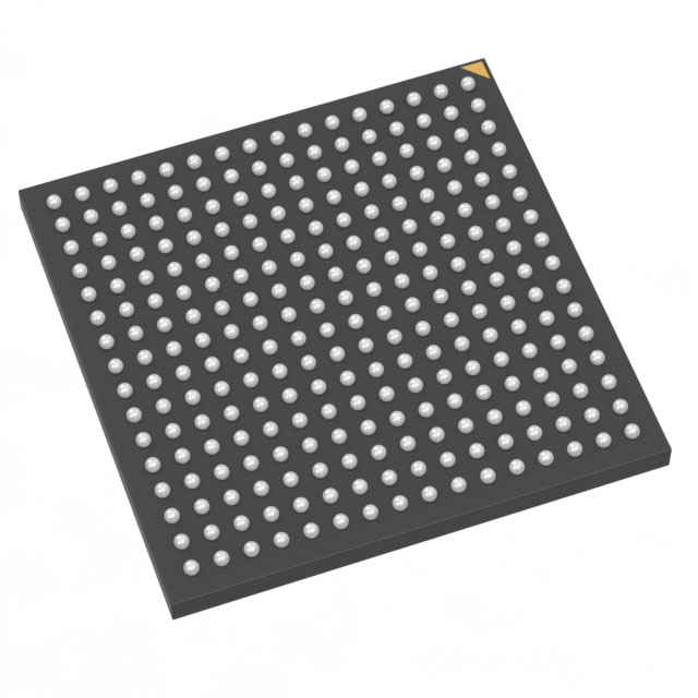
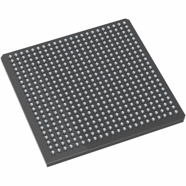
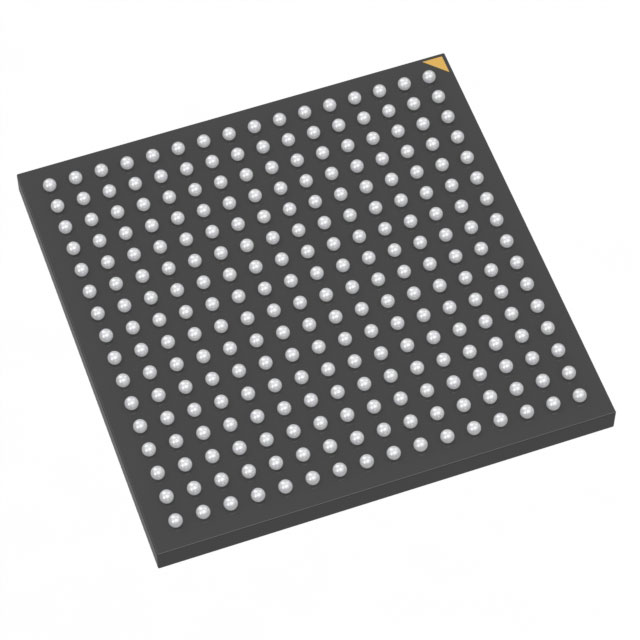
ORCA® 4 Field Programmable Gate Array (FPGA) IC 278 75776 4992 680-BBGA |
|---|---|
| Quantity | 75 Available (as of October 8, 2026) |

| Product Category | Field Programmable Gate Array (FPGA) |
|---|---|
| Manufacturer | Lattice Semiconductor Corporation |
| Manufacturing Status | Obsolete |
| Manufacturer Standard Lead Time | Contact Us |
| Datasheet |
Specifications & Environmental
| Device Package | 680-FPBGA (35x35) | Grade | Commercial | Operating Temperature | 0°C – 70°C | ||
|---|---|---|---|---|---|---|---|
| Package / Case | 680-BBGA | Number of I/O | 278 | Voltage | 1.425 V - 3.6 V | ||
| Mounting Method | Surface Mount | RoHS Compliance | Unknown | REACH Compliance | REACH Unaffected | ||
| Moisture Sensitivity Level | 3 (168 Hours) | Number of LABs/CLBs | 624 | Number of Logic Elements/Cells | 4992 | ||
| Number of Gates | 397000 | ECCN | 3A991D | HTS Code | 8542.39.0001 | ||
| Qualification | N/A | Total RAM Bits | 75776 |
Overview of ORT8850L-2BMN680C – ORCA® 4 Field-Programmable Gate Array, 278 I/O, 680-BBGA
The ORT8850L-2BMN680C is an ORCA® 4 Field-Programmable System Chip (FPSC) combining FPGA logic with integrated high-speed backplane transceivers. It provides 4,992 logic elements, 278 user I/Os and an embedded high-speed interface designed for board- and backplane-level data transfer.
Built for communication and system-integration tasks, this commercial-grade device integrates an eight-channel SERDES (up to 850 Mbits/s per channel) with a full-duplex synchronous interface and built-in clock-and-data recovery. It ships in a compact 680-BBGA / 680-FPBGA (35×35) package and is RoHS compliant.
Key Features
- FPGA Logic — 4,992 logic elements providing programmable logic resources for protocol, framing, and custom interface functions.
- Embedded Memory — 75,776 bits of on-chip RAM (approximately 0.076 Mbits) for buffering, FIFOs and small data structures.
- High-Speed SERDES — Eight-channel backplane transceiver architecture with up to 850 Mbits/s per channel (6.8 Gbits/s aggregate) for high-throughput inter-board or backplane links.
- SONET and Framing Support — Integrated SONET scrambler/descrambler, pointer handling and framing logic; SONET functionality can be hidden for non-SONET use.
- Interface and Clocking — Full-duplex synchronous interface with built-in clock and data recovery simplifies multiboard clock domain design and reduces backplane signal count.
- Package & Mounting — 680-BBGA (supplier package: 680-FPBGA, 35×35 mm) optimized for surface-mount assembly.
- Power & Environment — Supported supply range 1.425 V to 3.6 V; commercial operating temperature 0 °C to 70 °C.
- Regulatory — RoHS compliant.
Typical Applications
- Backplane Networking: Terminate and route high-speed backplane links using the integrated eight-channel transceiver and SONET-capable framing logic.
- Multi-Board Systems: Implement clockless high-speed interfaces and clock/data recovery for inter-device communication across boards and backplanes.
- Protocol Bridging and Framing: Build protocol-independent framers, ATM/PoS interfaces or HDLC/IP framers using the programmable FPGA fabric and embedded logic.
- High-Speed Bus Bridging: Deploy the device as a configurable bridge (for example, multi-Gbit PCI bridging topologies) leveraging the aggregated 6.8 Gbits/s SERDES bandwidth.
Unique Advantages
- Integrated SERDES and FPGA Fabric: Combines eight high-speed transceiver channels with programmable logic to reduce external components and simplify system architecture.
- Aggregated Throughput: Up to 6.8 Gbits/s aggregate bandwidth when all eight channels are used, enabling high-capacity backplane and board-level links.
- Compact, High-Density Package: 680-BBGA / 680-FPBGA (35×35) delivers large I/O count (278 pins) and dense logic in a compact surface-mount footprint.
- Flexible Clocking: Built-in clock and data recovery and full-duplex synchronous interface reduce clock-domain complexity in multiboard systems.
- Commercial Temperature Range: Rated for 0 °C to 70 °C for a wide range of standard embedded and communications equipment deployments.
- Standards-Ready Framing: On-chip SONET scrambler/descrambler and framing primitives accelerate development of telecom-oriented interfaces while allowing non-SONET usage when needed.
Why Choose ORT8850L-2BMN680C?
The ORT8850L-2BMN680C positions itself as a versatile FPSC platform for designs that need a compact, programmable FPGA plus integrated high-speed transceivers. With 4,992 logic elements, 278 I/Os, and an eight-channel SERDES subsystem, it is suited to designers implementing backplane communications, protocol termination, and high-throughput bus bridging within a commercial temperature envelope.
Its combination of embedded memory, programmable fabric and dedicated SONET/framing capabilities reduces system-level complexity and BOM count while providing the deterministic interfaces required in communications and system-integration applications. RoHS compliance and a standardized 680-BBGA package support production-ready board designs.
Request a quote or submit a procurement inquiry to receive pricing and availability for ORT8850L-2BMN680C and to discuss how it fits your design requirements.




















Date Founded: 1983
Headquarters: Hillsboro, Oregon, USA
Employees: 1,000+
Revenue: $627.7 Million
Certifications and Memberships: ISO9001:2015, ISO14001:2015, IATF16949:2016


