
ORT8850L-3BMN680C
| Part Description |
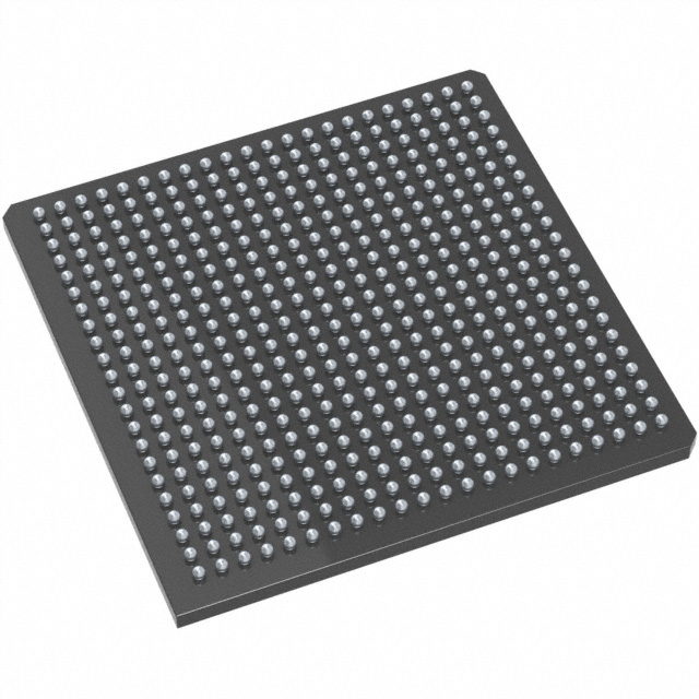
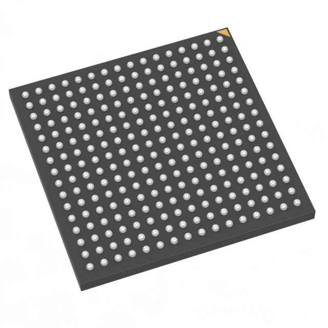
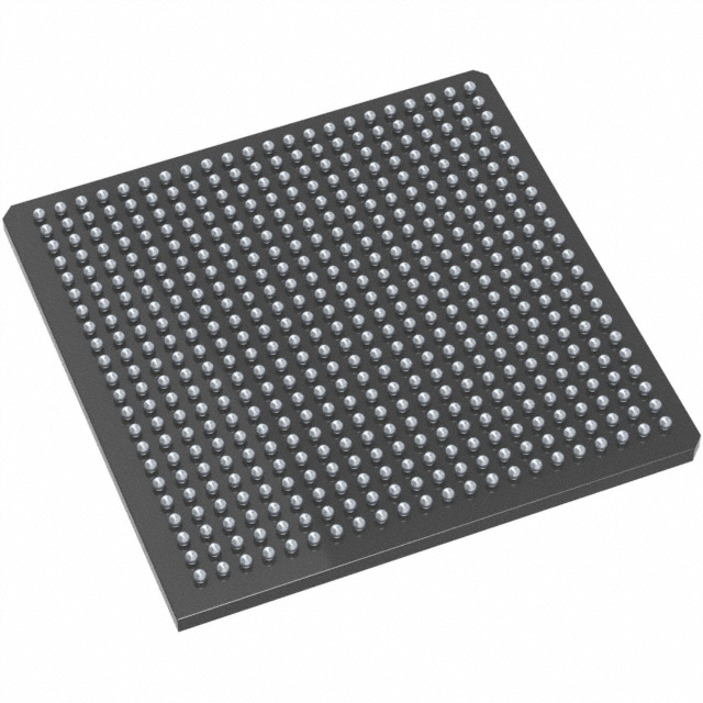
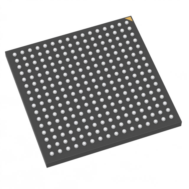
ORCA® 4 Field Programmable Gate Array (FPGA) IC 278 75776 4992 680-BBGA |
|---|---|
| Quantity | 454 Available (as of October 8, 2026) |

| Product Category | Field Programmable Gate Array (FPGA) |
|---|---|
| Manufacturer | Lattice Semiconductor Corporation |
| Manufacturing Status | Obsolete |
| Manufacturer Standard Lead Time | Contact Us |
| Datasheet |
Specifications & Environmental
| Device Package | 680-FPBGA (35x35) | Grade | Commercial | Operating Temperature | 0°C – 70°C | ||
|---|---|---|---|---|---|---|---|
| Package / Case | 680-BBGA | Number of I/O | 278 | Voltage | 1.425 V - 3.6 V | ||
| Mounting Method | Surface Mount | RoHS Compliance | Unknown | REACH Compliance | REACH Unaffected | ||
| Moisture Sensitivity Level | 3 (168 Hours) | Number of LABs/CLBs | 624 | Number of Logic Elements/Cells | 4992 | ||
| Number of Gates | 397000 | ECCN | 3A991D | HTS Code | 8542.39.0001 | ||
| Qualification | N/A | Total RAM Bits | 75776 |
Overview of ORT8850L-3BMN680C – ORCA® 4 Field Programmable Gate Array (FPGA) IC 278 75776 4992 680-BBGA
The ORT8850L-3BMN680C is a Field-Programmable System Chip (FPSC) from the ORCA ORT8850 family that combines FPGA logic with an integrated eight-channel backplane transceiver. Built on Lattice's Series 4 reconfigurable embedded System-on-a-Chip architecture, this device targets applications requiring programmable logic integrated with high-speed serial backplane connectivity.
Typical use cases include network termination and backplane interfacing, multiboard high-speed link implementations, and configurable protocol framing where a compact, surface-mount 680-pin FPBGA package and a broad I/O count are required.
Key Features
- Programmable Logic Approximately 4,992 logic elements (624 PFUs) for user logic and custom hardware implementation.
- Embedded Memory Approximately 75,776 bits of on-chip RAM to support frame buffers, packet processing, and user logic storage.
- High-Speed Backplane Transceiver Eight SERDES channels, each capable of up to 850 Mbits/s (aggregate up to 6.8 Gbits/s), with a full-duplex synchronous interface and built-in Clock and Data Recovery (CDR).
- I/O Density 278 user I/Os to support wide parallel interfaces and flexible board-level connectivity.
- System Gate Count Approximately 397,000 system gates providing the available logic resource sizing for system-level functions.
- Package & Mounting 680-FPBGA (35 × 35 mm) package, surface-mount assembly for compact board layouts.
- Power & Voltage Supported supply range from 1.425 V to 3.6 V for integration into varied power domains.
- Operating Range & Grade Commercial grade operation from 0 °C to 70 °C.
- Standards & Compliance RoHS compliant.
- Design Ecosystem Datasheet references ispLEVER development system and an FPSC design kit for design, configuration and integration workflows.
Typical Applications
- Backplane Networking & Termination Use the integrated eight-channel transceiver and SONET/SDH framing capabilities to implement backplane network termination and overhead handling.
- Multiboard High-Speed Links Clockless high-speed interface and on-chip CDR simplify clock domain management across boards and reduce backplane signal count.
- Protocol Framing & Custom Interfaces Combine FPGA logic with embedded transceivers to implement framers and protocol handling (for example ATM, PoS, or HDLC-like functions referenced in the ORT8850 family).
- High-Speed Bus Bridging Leverage the serial bandwidth to build high-throughput bridges between buses or subsystems (examples provided in product literature include PCI-to-PCI bridging).
Unique Advantages
- Highly integrated FPSC: The device combines programmable FPGA logic with an eight-channel backplane transceiver, reducing component count and simplifying board-level integration.
- Deterministic serial bandwidth: Eight channels at up to 850 Mbits/s each provide up to 6.8 Gbits/s aggregate throughput for multi-lane links.
- Substantial I/O and logic capacity: 278 user I/Os and roughly 4,992 logic elements support complex interfacing and custom logic implementation on a single device.
- Compact FPBGA package: 680-ball FPBGA (35 × 35 mm) package supports high-density designs while maintaining a surface-mount assembly profile.
- Flexible power support: Wide supply range (1.425 V to 3.6 V) eases integration into systems with different core and I/O voltage domains.
- Design tool support referenced: Product documentation references ispLEVER and an FPSC design kit to assist development and integration.
Why Choose ORT8850L-3BMN680C?
The ORT8850L-3BMN680C positions itself as an integrated solution for designers who need programmable FPGA resources alongside robust, multi-channel serial backplane connectivity. Its combination of approximately 4,992 logic elements, 278 I/Os, and eight SERDES channels makes it well suited for network-facing modules, backplane interconnects, and configurable protocol termination implementations in commercial-temperature systems.
With a compact 680-FPBGA package, broad supply voltage support, and RoHS compliance, this device offers a balanced mix of logic capacity, I/O density, and serial bandwidth for systems that require embedded framing, clock recovery, and on-chip protocol handling as described in the ORT8850 family documentation.
Request a quote or submit a product inquiry to obtain pricing, availability, and lead-time information for the ORT8850L-3BMN680C.




















Date Founded: 1983
Headquarters: Hillsboro, Oregon, USA
Employees: 1,000+
Revenue: $627.7 Million
Certifications and Memberships: ISO9001:2015, ISO14001:2015, IATF16949:2016


