
XC2V1000-5FF896I
| Part Description |
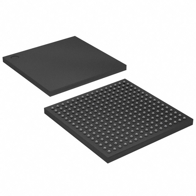
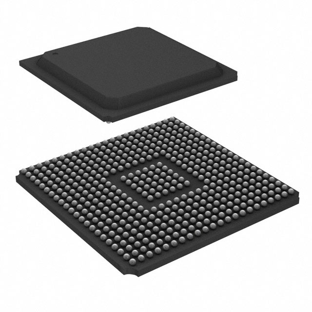
Virtex®-II Field Programmable Gate Array (FPGA) IC 432 737280 896-BBGA, FCBGA |
|---|---|
| Quantity | 570 Available (as of June 15, 2026) |

| Product Category | Field Programmable Gate Array (FPGA) |
|---|---|
| Manufacturer | AMD |
| Manufacturing Status | Obsolete |
| Manufacturer Standard Lead Time | Contact Us |
| Datasheet |
Specifications & Environmental
| Device Package | 896-FCBGA (31x31) | Grade | Industrial | Operating Temperature | -40°C – 100°C | ||
|---|---|---|---|---|---|---|---|
| Package / Case | 896-BBGA, FCBGA | Number of I/O | 432 | Voltage | 1.425 V - 1.575 V | ||
| Mounting Method | Surface Mount | RoHS Compliance | RoHS non-compliant | REACH Compliance | REACH Unaffected | ||
| Moisture Sensitivity Level | 4 (72 Hours) | Number of LABs/CLBs | 1280 | Number of Logic Elements/Cells | 11520 | ||
| Number of Gates | 1000000 | ECCN | 3A991D | HTS Code | 8542.39.0001 | ||
| Qualification | N/A | Total RAM Bits | 737280 |
Overview of XC2V1000-5FF896I – Virtex®-II Field Programmable Gate Array (FPGA) IC 432 737280 896-BBGA, FCBGA
The XC2V1000-5FF896I is a Virtex®-II platform FPGA supplied in an 896-ball flip-chip BGA (31×31) package. It provides 11,520 logic elements, approximately 0.74 Mbits of embedded RAM, and 432 user I/Os, making it suitable for industrial embedded systems that require flexible, reprogrammable logic with substantial on-chip memory and I/O density.
Designed for surface-mount assembly and rated for industrial temperatures (–40 °C to 100 °C) with a core supply range of 1.425 V to 1.575 V, this device is intended for applications that need a balance of logic capacity, memory resources, and robust I/O connectivity.
Key Features
- Logic Capacity — 11,520 logic elements providing programmable resources for custom digital functions and glue logic.
- Embedded Memory — Total on-chip RAM of 737,280 bits (approximately 0.74 Mbits) for embedded buffering, FIFOs, and local storage.
- I/O Density — 432 user I/O pins to support broad external interfacing and high-pin-count designs.
- System Gate Scale — Approximately 1,000,000 system gates for medium-density integration.
- Package & Mounting — 896-ball FCBGA package (31×31) optimized for surface-mount PCB assembly.
- Industrial Temperature & Supply — Rated for –40 °C to 100 °C operation with a core voltage range of 1.425 V to 1.575 V.
- Platform Series Features — Built on the Virtex-II platform; series-level features include SelectRAM memory hierarchy, dedicated 18-bit × 18-bit multiplier blocks, Digital Clock Manager (DCM) clock resources, and high-performance I/O standards as documented in the Virtex-II data volume.
- Regulatory — RoHS compliant for lead-free assembly compatibility.
Typical Applications
- Memory Interface and Bridge Designs — Use the device where on-chip memory and the Virtex-II platform’s external DRAM/SDRAM interface support are required for buffering and protocol bridging.
- Signal Processing and Arithmetic Acceleration — Leverage embedded RAM and the platform’s multiplier resources to implement fixed-point DSP blocks and custom arithmetic pipelines.
- High-Density I/O Aggregation — Deploy in systems needing large numbers of parallel I/Os for data acquisition, protocol conversion, or multi-channel sensor aggregation.
- Embedded System Glue Logic — Implement control, timing, and custom peripheral interfaces where reprogrammability and moderate logic capacity simplify BOM and design changes.
Unique Advantages
- Balanced Logic and Memory — 11,520 logic elements paired with approximately 0.74 Mbits of RAM offers a practical mix for mid-range custom logic and buffering without external SRAM dependence.
- High I/O Count — 432 user I/Os reduce the need for external multiplexing and enable direct connections to multiple peripherals or parallel data streams.
- Industrial Operational Range — Specified for –40 °C to 100 °C operation, supporting deployment in industrial environments.
- Surface-Mount, High-Density Package — 896-FCBGA (31×31) package supports compact board layouts and high-density system integration.
- Platform-Level Tool Support — As part of the Virtex-II family, the device is documented within the Virtex-II product specification and supported by the platform’s development resources.
- RoHS Compliance — Meets environmental requirements for lead-free assembly workflows.
Why Choose XC2V1000-5FF896I?
The XC2V1000-5FF896I positions itself as a reliable mid-range FPGA solution for industrial embedded designs that require a blend of programmable logic, embedded memory, and high I/O capacity. Its Virtex-II platform heritage brings documented architecture features—such as SelectRAM resources and dedicated multiplication blocks—that ease implementation of memory-intensive and arithmetic-heavy functions.
This device is well suited to engineers and procurement teams seeking a reprogrammable, industrial-grade FPGA in a compact FCBGA package, offering predictable supply voltage and temperature specifications along with RoHS compliance and platform-level documentation for design and verification.
Request a quote or submit an inquiry to receive availability, pricing, and volume lead-time information for the XC2V1000-5FF896I.


Date Founded: 1969
Headquarters: Santa Clara, California, USA
Employees: 25,000+
Revenue: $22.68 Billion
Certifications and Memberships: ISO9001:2015, RoHS, REACH


