
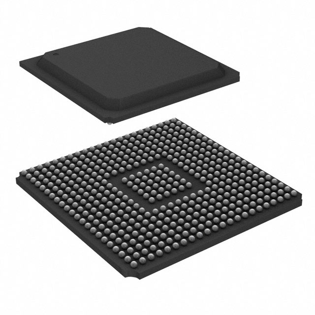
XC2V1000-5FG256C
| Part Description |
Virtex®-II Field Programmable Gate Array (FPGA) IC 172 737280 256-BGA |
|---|---|
| Quantity | 1,941 Available (as of June 14, 2026) |

| Product Category | Field Programmable Gate Array (FPGA) |
|---|---|
| Manufacturer | AMD |
| Manufacturing Status | Obsolete |
| Manufacturer Standard Lead Time | Contact Us |
| Datasheet |
Specifications & Environmental
| Device Package | 256-FBGA (17x17) | Grade | Commercial | Operating Temperature | 0°C – 85°C | ||
|---|---|---|---|---|---|---|---|
| Package / Case | 256-BGA | Number of I/O | 172 | Voltage | 1.425 V - 1.575 V | ||
| Mounting Method | Surface Mount | RoHS Compliance | RoHS non-compliant | REACH Compliance | REACH Unaffected | ||
| Moisture Sensitivity Level | 3 (168 Hours) | Number of LABs/CLBs | 1280 | Number of Logic Elements/Cells | 11520 | ||
| Number of Gates | 1000000 | ECCN | 3A001A7B | HTS Code | 8542.39.0001 | ||
| Qualification | N/A | Total RAM Bits | 737280 |
Overview of XC2V1000-5FG256C – Virtex®-II Field Programmable Gate Array (FPGA) IC 172 737280 256-BGA
The XC2V1000-5FG256C is a Virtex®-II platform field programmable gate array offering a balance of programmable logic, embedded memory and flexible I/O for mid-range designs. It provides a compact 256-ball BGA footprint with surface-mount assembly and features suited to designs that require on-chip RAM, dedicated multiplier blocks and a sizeable number of I/O pins.
Designed for commercial-grade applications, the device targets engineers building systems that need reprogrammable logic, on-chip memory and configurable interfaces while operating within a 1.425 V to 1.575 V supply range and a 0 °C to 85 °C ambient range.
Key Features
- Programmable Logic 11,520 logic elements providing fabric for implementing custom digital functions and control logic.
- Embedded Memory Approximately 0.737 Mbits of on-chip RAM (737,280 total bits) for data buffering, FIFOs and state storage.
- Dedicated Arithmetic Built-in 18-bit × 18-bit multiplier blocks for efficient implementation of DSP and arithmetic-intensive functions (as described in the Virtex‑II architecture).
- Clock Management Architecture-level support for Digital Clock Manager (DCM) modules to manage clock de-skew, frequency synthesis and phase shifts (Virtex‑II platform feature).
- I/O Capacity and Flexibility 172 user I/O pins in the 256-BGA package to interface with external devices and memories; supports high-performance signaling modes described for the Virtex‑II family.
- Package and Mounting 256-BGA (supplier device package: 256-FBGA 17 × 17) optimized for surface-mount assembly in compact board designs.
- Power and Operating Range Core supply 1.425 V to 1.575 V; commercial operating temperature from 0 °C to 85 °C.
- Standards and Compliance RoHS-compliant manufacturing status for regulatory and environmental alignment.
Typical Applications
- High-bandwidth memory interfaces Use the device’s configurable I/O and on-chip memory to implement SDR/DDR interface logic and memory controllers described in the Virtex‑II platform.
- Signal processing and DSP blocks Leverage the dedicated 18×18 multipliers and embedded RAM for filters, transforms and arithmetic acceleration.
- Custom protocol bridging Implement protocol converters and bespoke bus logic using the programmable fabric and 172 I/O pins to connect diverse peripherals.
- Embedded control and glue logic Replace complex discrete logic with consolidated programmable logic and on-chip memory to simplify board-level design.
Unique Advantages
- Balanced logic and memory mix: 11,520 logic elements paired with approximately 0.737 Mbits of embedded RAM enable mid-range designs to integrate control, buffering and data-path functions on a single device.
- Hardware-accelerated arithmetic: On-die 18×18 multipliers reduce the need for external DSP components when implementing multiply-intensive algorithms.
- Flexible I/O in a compact package: 172 user I/Os in a 256-BGA (256-FBGA 17×17) form factor lets designers fit substantial interface capability into space-constrained PCBs.
- Platform-level clock flexibility: Support for DCM modules enables precise clock management and phase control for multi-clock designs (Virtex‑II platform feature).
- Commercial temperature and RoHS compliance: Specified for 0 °C to 85 °C operation and RoHS-compliant, aligning with standard commercial product requirements.
Why Choose XC2V1000-5FG256C?
The XC2V1000-5FG256C positions itself as a practical Virtex‑II FPGA choice for engineers who need a combination of programmable logic, embedded RAM and arithmetic resources in a compact 256-BGA package. Its 11,520 logic elements, dedicated multiplier blocks and 172 I/Os provide the building blocks for mid-range embedded systems, interface logic and signal-processing functions.
With a defined supply range and commercial temperature grade, plus RoHS compliance, this device is suited to production designs where reproducible electrical requirements and regulatory alignment matter. The Virtex‑II platform features referenced in the datasheet—such as SelectRAM resources and clock management—support scalable designs and established development flows.
If you would like pricing or availability, request a quote or submit a product inquiry to receive details and lead-time information for the XC2V1000-5FG256C.


Date Founded: 1969
Headquarters: Santa Clara, California, USA
Employees: 25,000+
Revenue: $22.68 Billion
Certifications and Memberships: ISO9001:2015, RoHS, REACH


