
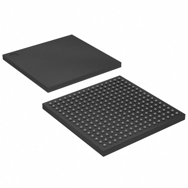
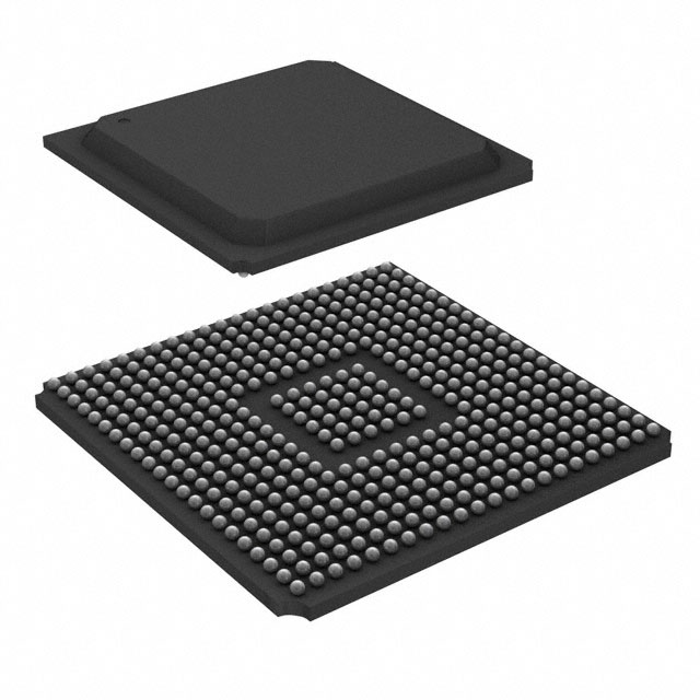
XC2V1000-5FGG256I
| Part Description |
Virtex®-II Field Programmable Gate Array (FPGA) IC 172 737280 256-BGA |
|---|---|
| Quantity | 830 Available (as of June 15, 2026) |
| Product Category | Field Programmable Gate Array (FPGA) |
|---|---|
| Manufacturer | AMD |
| Manufacturing Status | Obsolete |
| Manufacturer Standard Lead Time | Contact Us |
| Datasheet |
Specifications & Environmental
| Device Package | 256-FBGA (17x17) | Grade | Industrial | Operating Temperature | -40°C – 100°C | ||
|---|---|---|---|---|---|---|---|
| Package / Case | 256-BGA | Number of I/O | 172 | Voltage | 1.425 V - 1.575 V | ||
| Mounting Method | Surface Mount | RoHS Compliance | Unknown | REACH Compliance | REACH Unaffected | ||
| Moisture Sensitivity Level | 3 (168 Hours) | Number of LABs/CLBs | 1280 | Number of Logic Elements/Cells | 11520 | ||
| Number of Gates | 1000000 | ECCN | 3A001A7B | HTS Code | 8542.39.0001 | ||
| Qualification | N/A | Total RAM Bits | 737280 |
Overview of XC2V1000-5FGG256I – Virtex®-II FPGA, 256-BGA (Industrial)
The XC2V1000-5FGG256I is a Virtex®-II Field Programmable Gate Array (FPGA) provided by AMD, offered in a 256-ball BGA package. It delivers a balanced combination of programmable logic, embedded memory, and I/O connectivity aimed at mid-density FPGA applications.
Built on the Virtex-II platform architecture, the device targets designs that need on-chip RAM, dedicated arithmetic resources, and flexible I/O while operating across an industrial temperature range and a narrow core voltage window for controlled power delivery.
Key Features
- Logic Capacity Approximately 11,520 logic elements and about 1,000,000 system gates, providing a mid-range fabric for custom digital logic implementations.
- Configurable Logic Blocks 1,280 CLB resources (as specified) to structure and map user logic across the device.
- Embedded Memory Approximately 0.737 Mbits of on-chip RAM (737,280 total RAM bits) for block and distributed memory needs within the design.
- Dedicated Arithmetic Virtex-II platform includes 18-bit × 18-bit multiplier resources for hardware-accelerated multiply operations (platform feature).
- I/O Resources 172 user I/Os available on the 256-BGA package to interface with external devices and buses.
- Clock and Timing Platform-level clock management features (Digital Clock Manager and global clock buffers) designed to support precise clock distribution and de-skew in complex designs.
- Package and Mounting 256-BGA (supplier package: 256-FBGA, 17×17) in a surface-mount form factor for PCB assembly.
- Power Supply Core voltage supply range from 1.425 V to 1.575 V to match regulated FPGA power rails.
- Temperature and Grade Industrial grade device with an operating temperature range of −40 °C to 100 °C.
- Compliance RoHS compliant for environmental and lead-free assembly considerations.
Typical Applications
- Memory Interface and Control Use the device’s embedded memory and platform memory hierarchy to implement DRAM/SRAM interface logic and buffer control functions.
- Signal Processing Leverage the device’s embedded RAM and multiplier resources for fixed-point DSP functions, packet processing, and data-path acceleration.
- Custom Logic and Glue Mid-density logic capacity and flexible I/O make the FPGA suitable for glue logic, protocol conversion, and custom peripheral controllers in embedded systems.
- Timing-Critical Designs Platform clock management capabilities support applications requiring precise clock distribution and phase control across multiple clock domains.
Unique Advantages
- Balanced Logic and Memory Combines approximately 11,520 logic elements with ~0.737 Mbits of embedded RAM to support both control logic and data buffering on-chip, reducing external memory dependencies.
- Dedicated Arithmetic Resources Includes platform-level 18×18 multiplier blocks to accelerate multiply-intensive algorithms without consuming general-purpose logic.
- Flexible I/O Count 172 user I/Os in a compact 256-BGA footprint enable integration with numerous peripherals and board-level interfaces while keeping PCB area modest.
- Industrial Temperature Range Rated from −40 °C to 100 °C for deployment in industrial environments where extended temperature operation is required.
- Controlled Core Voltage Narrow supply range (1.425 V–1.575 V) supports precise power sequencing and predictable power delivery for reliable operation.
- RoHS Compliant Manufactured to meet RoHS requirements for lead-free assembly and regulatory conformity.
Why Choose XC2V1000-5FGG256I?
The XC2V1000-5FGG256I positions itself as a mid-density Virtex®-II FPGA option that blends programmable logic, embedded memory, and dedicated arithmetic blocks suitable for a range of embedded and signal-processing tasks. Its industrial temperature rating and RoHS compliance make it suitable for long-life and environmentally compliant designs.
This device is appropriate for engineers seeking a compact BGA package with a defined I/O count and on-chip resources that reduce external component count and simplify board-level design. The combination of core voltage specification, package, and platform-level features supports scalable designs where predictable power and timing behavior are important.
If you would like pricing, availability, or to request a quote for XC2V1000-5FGG256I, submit an inquiry or quote request and our team will respond with product and procurement details.


Date Founded: 1969
Headquarters: Santa Clara, California, USA
Employees: 25,000+
Revenue: $22.68 Billion
Certifications and Memberships: ISO9001:2015, RoHS, REACH


