
XC2V1000-6BGG575C
| Part Description |
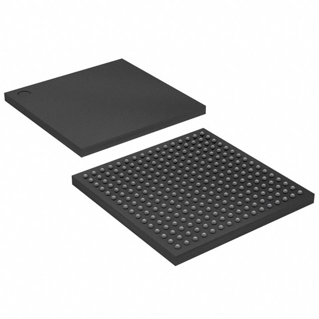
Virtex®-II Field Programmable Gate Array (FPGA) IC 328 737280 575-BBGA |
|---|---|
| Quantity | 97 Available (as of June 15, 2026) |

| Product Category | Field Programmable Gate Array (FPGA) |
|---|---|
| Manufacturer | AMD |
| Manufacturing Status | Obsolete |
| Manufacturer Standard Lead Time | Contact Us |
| Datasheet |
Specifications & Environmental
| Device Package | 575-BGA (31x31) | Grade | Commercial | Operating Temperature | 0°C – 85°C | ||
|---|---|---|---|---|---|---|---|
| Package / Case | 575-BBGA | Number of I/O | 328 | Voltage | 1.425 V - 1.575 V | ||
| Mounting Method | Surface Mount | RoHS Compliance | Unknown | REACH Compliance | REACH Unaffected | ||
| Moisture Sensitivity Level | 3 (168 Hours) | Number of LABs/CLBs | 1280 | Number of Logic Elements/Cells | 11520 | ||
| Number of Gates | 1000000 | ECCN | 3A991D | HTS Code | 8542.39.0001 | ||
| Qualification | N/A | Total RAM Bits | 737280 |
Overview of XC2V1000-6BGG575C – Virtex®-II Field Programmable Gate Array (FPGA) IC 328 737280 575-BBGA
The XC2V1000-6BGG575C is a Virtex®-II platform field programmable gate array designed for mid-range programmable-logic applications. This commercial-grade, surface-mount FPGA integrates approximately 11,520 logic elements, roughly 1,000,000 system gates and approximately 0.74 Mbits of embedded RAM to support complex logic and memory-intense functions.
Targeted at designs that require flexible I/O and on-chip arithmetic and clock management resources, the device delivers a balanced mix of logic density, I/O capability and on-chip memory while operating from a 1.425 V to 1.575 V supply in a compact 575-BBGA (31×31) package.
Key Features
- Logic Capacity Approximately 11,520 logic elements (11520 logic cells) and about 1,000,000 gates provide mid-range programmable logic for combinational and sequential designs.
- Embedded Memory Approximately 737,280 bits (≈0.74 Mbits) of on-chip RAM for buffering, FIFOs and small data structures within the FPGA fabric.
- I/O Resources 328 user I/O pins support a wide range of external interfaces and peripherals while enabling dense board-level connectivity.
- Arithmetic and DSP Series-level features include dedicated 18-bit × 18-bit multiplier blocks useful for multiply-accumulate and signal-processing functions.
- Clock Management Supports Digital Clock Manager (DCM) functionality from the Virtex®-II platform for clock de-skew, synthesis and phase adjustments when used in designs leveraging platform features.
- Package & Mounting 575-BBGA (31×31) ball-grid array in a surface-mount package for compact, high-density board layouts.
- Power & Supply Operates from a core supply range of 1.425 V to 1.575 V, enabling predictable power budgeting within the specified range.
- Operating Range Commercial temperature rating from 0 °C to 85 °C for standard ambient operating conditions.
- Compliance RoHS compliant, meeting common lead-free requirements for electronic assemblies.
Typical Applications
- Communications Equipment Implements protocol bridging, packet processing, and memory-interface logic using the device’s combination of logic, embedded RAM and high I/O count.
- DSP and Signal Processing Leverages on-chip multiplier blocks and embedded RAM to accelerate filtering, transforms and other arithmetic-heavy functions.
- Prototyping and System Integration Serves as a flexible platform for validating custom logic, integrating peripherals and interfacing with external memory devices.
- Industrial Control Handles mid-complexity control, sequencing and I/O aggregation tasks within commercial-temperature systems.
Unique Advantages
- Balanced Logic and Memory Combines roughly 11,520 logic elements with approximately 0.74 Mbits of embedded RAM to support mixed-control and data-path designs without immediate external memory dependence.
- High I/O Density 328 available I/Os let designers implement multiple parallel interfaces and expand board-level connectivity while maintaining a single-package solution.
- On-Chip Arithmetic Blocks Dedicated 18×18 multipliers simplify implementation of DSP kernels and offload compute from external processors.
- Compact, Surface-Mount Package 575-BBGA (31×31) offers a space-efficient footprint for designs where board area is a consideration.
- Predictable Power Envelope Defined core supply range (1.425 V–1.575 V) supports consistent power planning and voltage rail design.
- Regulatory Compatibility RoHS compliance supports lead-free assembly requirements and common environmental regulations.
Why Choose XC2V1000-6BGG575C?
The XC2V1000-6BGG575C positions itself as a mid-range Virtex®-II FPGA option that balances programmable logic capacity, embedded memory and a substantial I/O complement in a compact 575-BBGA surface-mount package. Its combination of approximately 11,520 logic elements, roughly 1,000,000 gates and approximately 0.74 Mbits of on-chip RAM makes it well suited to designs that need moderate logic density with on-board memory and DSP support while operating within standard commercial temperature ranges.
For engineering teams and procurement groups building communication, DSP, prototyping or industrial-control systems, this device delivers a robust platform-level feature set from the Virtex®-II family with predictable power and package characteristics and RoHS compliance for lead-free assembly workflows.
Request a quote or submit an inquiry to obtain pricing and availability for the XC2V1000-6BGG575C. Include your quantity and required lead time for a tailored response.


Date Founded: 1969
Headquarters: Santa Clara, California, USA
Employees: 25,000+
Revenue: $22.68 Billion
Certifications and Memberships: ISO9001:2015, RoHS, REACH


