
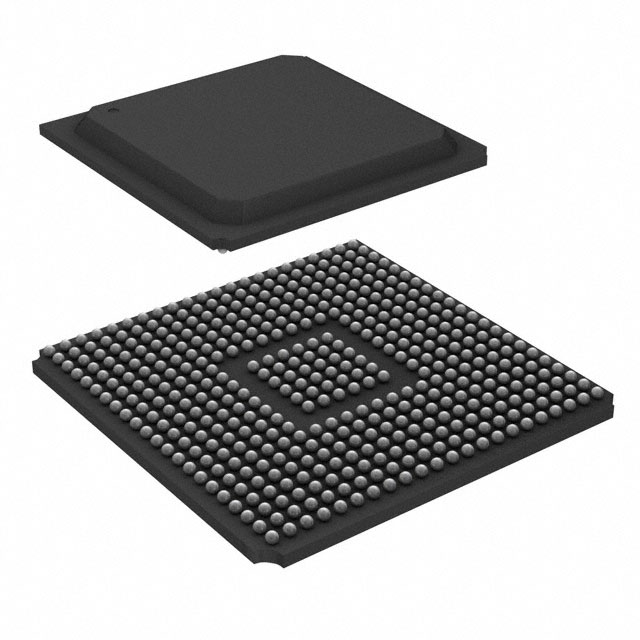
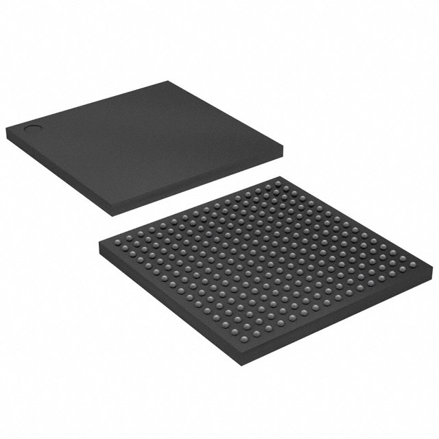
XC2V1000-5FGG256C
| Part Description |
Virtex®-II Field Programmable Gate Array (FPGA) IC 172 737280 256-BGA |
|---|---|
| Quantity | 824 Available (as of June 10, 2026) |

| Product Category | Field Programmable Gate Array (FPGA) |
|---|---|
| Manufacturer | AMD |
| Manufacturing Status | Obsolete |
| Manufacturer Standard Lead Time | Contact Us |
| Datasheet |
Specifications & Environmental
| Device Package | 256-FBGA (17x17) | Grade | Commercial | Operating Temperature | 0°C – 85°C | ||
|---|---|---|---|---|---|---|---|
| Package / Case | 256-BGA | Number of I/O | 172 | Voltage | 1.425 V - 1.575 V | ||
| Mounting Method | Surface Mount | RoHS Compliance | Unknown | REACH Compliance | REACH Unaffected | ||
| Moisture Sensitivity Level | 3 (168 Hours) | Number of LABs/CLBs | 1280 | Number of Logic Elements/Cells | 11520 | ||
| Number of Gates | 1000000 | ECCN | 3A001A7B | HTS Code | 8542.39.0001 | ||
| Qualification | N/A | Total RAM Bits | 737280 |
Overview of XC2V1000-5FGG256C – Virtex®-II Field Programmable Gate Array (FPGA) IC 172 737280 256-BGA
The XC2V1000-5FGG256C is a commercial-grade Virtex®-II platform FPGA offered by AMD. It delivers a reprogrammable logic fabric with 11,520 logic elements, embedded memory, and a 172-pin I/O count in a 256-ball fine-pitch BGA package suitable for surface-mount assembly.
Designed for applications that require flexible, high-density programmable logic with substantial on-chip RAM and a broad set of I/O capabilities, this device balances integration and I/O flexibility while operating from a 1.425 V to 1.575 V supply within a 0 °C to 85 °C commercial temperature range.
Key Features
- Logic Capacity Approximately 11,520 logic elements providing reprogrammable logic resources for custom digital functions and system integration.
- Embedded Memory Approximately 0.74 Mbits of on-chip RAM (737,280 total RAM bits) for data buffering, FIFOs, and embedded storage.
- I/O Count & Package 172 user I/Os in a 256-ball fine-pitch BGA package (256-FBGA, 17×17); surface-mount mounting type for compact board designs.
- Gate Equivalent Listed at 1,000,000 gates, enabling mid-range system integration and logic consolidation.
- Power and Operating Range Core supply 1.425 V to 1.575 V and commercial operating temperature from 0 °C to 85 °C.
- Memory and Arithmetic Architecture (Virtex-II) Series-level features include a SelectRAM memory hierarchy and dedicated 18 × 18 multipliers for efficient arithmetic implementation.
- Clocking and Timing (Virtex-II) Series-level clock management capabilities such as Digital Clock Manager (DCM) modules and global clock buffers to support precise clocking architectures.
- I/O Technology (Virtex-II) Series-level SelectIO features and Digitally Controlled Impedance (DCI) options for flexible interfacing and on-chip termination where applicable.
- Compliance RoHS compliant.
Typical Applications
- Memory Interface Prototyping Use for designs requiring on-chip RAM and series-level high-performance external memory interfaces such as SDR/DDR SDRAM and specialized SRAM variants.
- Digital Signal and Arithmetic Acceleration Leverage dedicated multiplier blocks and abundant logic elements for DSP blocks, filtering, and arithmetic pipelines.
- Custom I/O and Protocol Bridging Deploy where flexible I/O counts and SelectIO capabilities are needed to connect diverse peripherals or implement custom bus bridges.
- Embedded System Glue Logic Integrate complex control logic, state machines, and buffering functions to reduce board-level BOM and simplify system architecture.
Unique Advantages
- High-density reprogrammable logic: 11,520 logic elements and 1,000,000 gate equivalence enable consolidation of discrete logic and embedded subsystems into a single device.
- Substantial on-chip RAM: Approximately 0.74 Mbits of embedded memory reduces dependence on external memory for moderate buffering and storage needs.
- Flexible I/O and package: 172 user I/Os in a compact 256-FBGA (17×17) surface-mount package support complex interfacing while keeping PCB area small.
- Clock and arithmetic resources: Series-level Digital Clock Manager and dedicated multipliers simplify implementation of precise timing and compute-intensive functions.
- Regulatory and assembly readiness: RoHS compliance and surface-mount BGA packaging support modern manufacturing and environmental requirements.
- Commercial temperature rating: Specified for 0 °C to 85 °C environments, appropriate for a wide range of commercial and consumer electronics designs.
Why Choose XC2V1000-5FGG256C?
The XC2V1000-5FGG256C delivers a balanced mix of logic density, embedded memory, and flexible I/O in a compact 256-FBGA package. Its Virtex®-II platform capabilities—such as SelectRAM memory hierarchy, dedicated multipliers, and clock management features—make it well suited for mid-range FPGA tasks where integration and adaptability are priorities.
This device is a fit for engineering teams that need reprogrammable logic to prototype or deploy custom digital functions, memory interfaces, and protocol bridging while maintaining a compact board footprint and RoHS-compliant manufacturing readiness.
If you would like pricing, availability, or to request a quote for XC2V1000-5FGG256C, please submit a quote request or contact sales to get started.


Date Founded: 1969
Headquarters: Santa Clara, California, USA
Employees: 25,000+
Revenue: $22.68 Billion
Certifications and Memberships: ISO9001:2015, RoHS, REACH


