
XC2V80-6FGG256C
| Part Description |
Virtex®-II Field Programmable Gate Array (FPGA) IC 120 147456 256-BGA |
|---|---|
| Quantity | 916 Available (as of June 16, 2026) |

| Product Category | Field Programmable Gate Array (FPGA) |
|---|---|
| Manufacturer | AMD |
| Manufacturing Status | Obsolete |
| Manufacturer Standard Lead Time | Contact Us |
| Datasheet |
Specifications & Environmental
| Device Package | 256-FBGA (17x17) | Grade | Commercial | Operating Temperature | 0°C – 85°C | ||
|---|---|---|---|---|---|---|---|
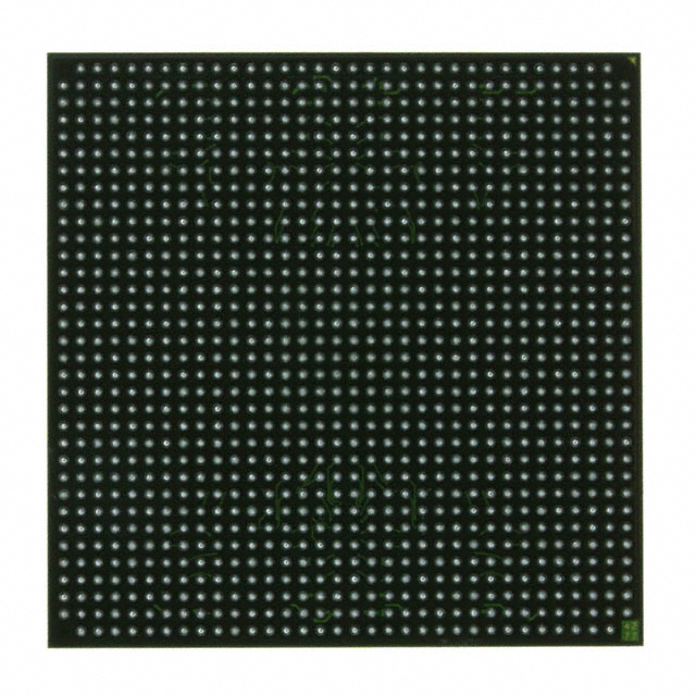
| Package / Case | 256-BGA | Number of I/O | 120 | Voltage | 1.425 V - 1.575 V | ||
| Mounting Method | Surface Mount | RoHS Compliance | Unknown | REACH Compliance | REACH Unaffected | ||
| Moisture Sensitivity Level | 3 (168 Hours) | Number of LABs/CLBs | 128 | Number of Logic Elements/Cells | 1152 | ||
| Number of Gates | 80000 | ECCN | EAR99 | HTS Code | 8542.39.0001 | ||
| Qualification | N/A | Total RAM Bits | 147456 |
Overview of XC2V80-6FGG256C – Virtex®-II FPGA, 256-BGA
The XC2V80-6FGG256C is a Virtex®-II field programmable gate array in a 256-ball fine-pitch BGA package. Built for commercial embedded and system designs, it combines programmable logic, on-chip memory, and flexible I/O to implement custom digital functions, memory interfaces, and timing-critical logic.
Designed around the Virtex-II platform architecture, this device targets applications that require mid-range gate density, dedicated embedded memory, and multi-standard I/O in a compact 17 × 17 mm FBGA footprint.
Key Features
- Logic Capacity — 1152 logic elements and 128 configurable logic blocks (CLBs) to implement custom logic, state machines, and control functions.
- Embedded Memory — 147,456 bits of on-chip RAM (approximately 0.144 Mbits) suitable for FIFOs, buffers, and small data stores.
- I/O Resources — 120 user I/Os provided on the 256-ball BGA package for interfacing to peripherals, memory, and external devices.
- Arithmetic & DSP — Virtex-II family features such as dedicated 18-bit × 18-bit multiplier resources for arithmetic acceleration are described in the Virtex-II data volume.
- Clock Management — The Virtex-II platform includes clock management features (Digital Clock Manager and global clock buffers) to support precise clock distribution and deskewing in complex designs.
- Power and Supply — Operates from a core voltage supply range of 1.425 V to 1.575 V, enabling integration into regulated power domains.
- Package — 256-FBGA (17 × 17 mm) package case suitable for surface-mount PCB assembly and compact system layouts.
- Operating Range — Commercial temperature grade rated for 0 °C to 85 °C.
- Regulatory — RoHS-compliant component, meeting common lead-free requirements for commercial assemblies.
Typical Applications
- Embedded Control — Implement custom control logic, state machines, and peripheral interfaces in compact embedded systems using the device's logic and I/O resources.
- Prototyping and Development — Rapid hardware prototyping where reprogrammability and a mid-range logic footprint accelerate iteration and validation.
- Memory Interface and Buffering — Use the on-chip RAM and abundant I/O for small buffering, FIFO implementations, and interfacing to external memory subsystems.
- Signal Processing Acceleration — Leverage the Virtex-II arithmetic resources for fixed-point multiply-accumulate blocks and other DSP building blocks described by the platform.
Unique Advantages
- Balanced Mid-Range Capacity: 1152 logic elements with 128 CLBs provide a compact yet capable fabric for medium-complexity designs without excess board-level area.
- Integrated On-Chip RAM: 147,456 bits of embedded RAM reduce external memory needs for control buffers and small data structures, simplifying BOM and layout.
- Flexible I/O Count: 120 user I/Os in a 256-BGA footprint enable dense peripheral and memory connectivity in space-constrained designs.
- Commercial Temperature Rating: 0 °C to 85 °C operation aligns with standard commercial applications and ensures predictable behavior across typical operating conditions.
- Compact Package: The 256-FBGA (17 × 17) package enables high pin count in a small PCB area, facilitating compact system integration.
- RoHS Compliant: Lead-free compliance simplifies integration into modern commercial product manufacturing flows.
Why Choose XC2V80-6FGG256C?
The XC2V80-6FGG256C delivers a practical balance of logic, on-chip RAM, and I/O in a compact 256-ball FBGA package for commercial embedded and system-level designs. It is suited to engineers who need reprogrammable logic with integrated memory and a sizeable I/O complement while maintaining a small PCB footprint.
Backed by the Virtex-II family architecture and documentation, this device is a strong option for mid-range designs requiring deterministic clock management, embedded arithmetic resources, and standard commercial operating conditions.
Request a quote or submit a purchase inquiry to get pricing and availability for the XC2V80-6FGG256C and include your intended quantities and delivery requirements.


Date Founded: 1969
Headquarters: Santa Clara, California, USA
Employees: 25,000+
Revenue: $22.68 Billion
Certifications and Memberships: ISO9001:2015, RoHS, REACH


