
XC2V8000-4FF1152I
| Part Description |
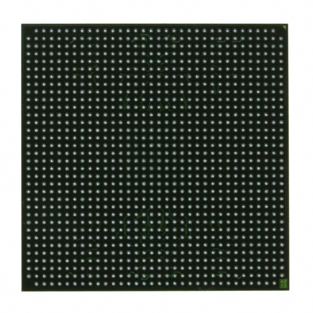
Virtex®-II Field Programmable Gate Array (FPGA) IC 824 3096576 1152-BBGA, FCBGA |
|---|---|
| Quantity | 963 Available (as of June 13, 2026) |

| Product Category | Field Programmable Gate Array (FPGA) |
|---|---|
| Manufacturer | AMD |
| Manufacturing Status | Obsolete |
| Manufacturer Standard Lead Time | Contact Us |
| Datasheet |
Specifications & Environmental
| Device Package | 1152-FCBGA (35x35) | Grade | Industrial | Operating Temperature | -40°C – 100°C | ||
|---|---|---|---|---|---|---|---|
| Package / Case | 1152-BBGA, FCBGA | Number of I/O | 824 | Voltage | 1.425 V - 1.575 V | ||
| Mounting Method | Surface Mount | RoHS Compliance | RoHS non-compliant | REACH Compliance | REACH Unaffected | ||
| Moisture Sensitivity Level | 4 (72 Hours) | Number of LABs/CLBs | 11648 | Number of Logic Elements/Cells | 104832 | ||
| Number of Gates | 8000000 | ECCN | 3A001A7A | HTS Code | 8542.39.0001 | ||
| Qualification | N/A | Total RAM Bits | 3096576 |
Overview of XC2V8000-4FF1152I – Virtex®-II FPGA, 1152-FCBGA, Industrial (824 I/O)
The XC2V8000-4FF1152I is a Virtex®-II Field Programmable Gate Array (FPGA) offered in a 1152-FCBGA (35×35) surface-mount package. It delivers large programmable logic capacity, extensive on-chip memory, and dense I/O for industrial-grade embedded and system-level designs.
Built on the Virtex-II platform architecture, this device targets applications that require substantial logic resources, flexible memory structures, and robust clocking and I/O options while operating over an industrial temperature range.
Key Features
- Core Logic Capacity 11,648 configurable logic blocks (CLBs) and 104,832 logic cells, representing approximately 8,000,000 system gates for complex logic integration.
- Embedded Memory Approximately 3.1 Mbits of on-chip RAM (3,096,576 total bits), implemented in 18-Kb block SelectRAM resources for dual-port and distributed memory requirements.
- Arithmetic and DSP Resources Series-level support for dedicated 18-bit × 18-bit multiplier blocks enables hardware-accelerated arithmetic and signal processing functions.
- Clock Management Virtex-II platform features include Digital Clock Manager (DCM) modules and global clock multiplexer buffers for flexible frequency synthesis and precise clock de-skew.
- I/O Density and Packaging 824 user I/Os in a 1152-BBGA FCBGA package (1152-FCBGA, 35×35), surface-mount mounting for high-density board designs.
- Voltage and Thermal Core supply range of 1.425 V to 1.575 V and rated operating temperature from −40 °C to 100 °C for industrial deployment.
- Standards and I/O Technology (Platform) Virtex-II platform-level I/O features include SelectIO technology and Digitally Controlled Impedance (DCI) for flexible interface standards and on-chip termination (series-level capability).
- Compliance RoHS compliant and specified as industrial grade.
- Development Ecosystem (Platform) Supported by the Virtex-II development flow and Xilinx Foundation/Alliance series development systems (platform-level support documented in the product family datasheet).
Typical Applications
- High-performance embedded systems — Implements complex custom logic and hardware accelerators using the large pool of CLBs and logic cells.
- Memory-interface designs — On-chip RAM and series-level DRAM/SRAM interface support enable high-bandwidth external memory controllers and buffering.
- Signal processing and DSP — Dedicated multiplier blocks and abundant logic resources support arithmetic heavy workloads and real-time processing.
- Industrial control and automation — Industrial temperature grading and comprehensive I/O count make the device suitable for demanding embedded control and I/O aggregation tasks.
Unique Advantages
- High programmable density: Large CLB and logic-cell counts let you consolidate multiple functions into a single FPGA, reducing board-level complexity.
- Substantial on-chip RAM: Approximately 3.1 Mbits of embedded memory enables deep buffering, large lookup tables, and efficient dual-port memory architectures.
- Flexible clocking: Platform Digital Clock Manager and global clock resources support precise timing control and complex multi-clock designs.
- Dense, flexible I/O: 824 user I/Os in a compact FCBGA package accommodate numerous peripherals and high-pin-count interfaces without external multiplexing.
- Industrial operating range: Specified −40 °C to 100 °C and RoHS compliance support deployment in industrial environments.
Why Choose XC2V8000-4FF1152I?
The XC2V8000-4FF1152I combines large programmable logic resources, significant embedded memory, and a high I/O count in a single industrial-grade FCBGA package. It is positioned for designers who need to implement complex logic, memory controllers, and arithmetic-intensive functions while meeting industrial temperature and mounting requirements.
This device benefits teams looking for scalability within the Virtex-II platform, leveraging platform-level features such as SelectRAM block memory, dedicated multipliers, and advanced clock management to accelerate time-to-deployment and simplify system integration.
If you would like pricing, lead time, or to request a formal quote for XC2V8000-4FF1152I, please submit a quote request or sales inquiry and our team will respond with the next steps.


Date Founded: 1969
Headquarters: Santa Clara, California, USA
Employees: 25,000+
Revenue: $22.68 Billion
Certifications and Memberships: ISO9001:2015, RoHS, REACH


