
XC4003-6PQ100C
| Part Description |
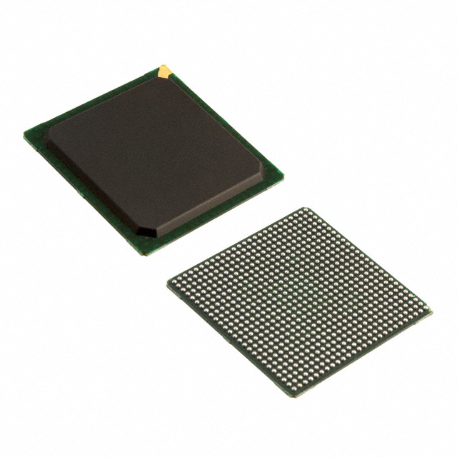
XC4000 Field Programmable Gate Array (FPGA) IC 77 3200 238 100-BQFP |
|---|---|
| Quantity | 819 Available (as of October 7, 2026) |

| Product Category | Field Programmable Gate Array (FPGA) |
|---|---|
| Manufacturer | AMD |
| Manufacturing Status | Obsolete |
| Manufacturer Standard Lead Time | Contact Us |
| Datasheet |
Specifications & Environmental
| Device Package | 100-PQFP (20x14) | Grade | Commercial | Operating Temperature | 0°C – 85°C | ||
|---|---|---|---|---|---|---|---|
| Package / Case | 100-BQFP | Number of I/O | 77 | Voltage | 4.75 V - 5.25 V | ||
| Mounting Method | Surface Mount | RoHS Compliance | RoHS non-compliant | REACH Compliance | REACH Unaffected | ||
| Moisture Sensitivity Level | 3 (168 Hours) | Number of LABs/CLBs | 100 | Number of Logic Elements/Cells | 238 | ||
| Number of Gates | 3000 | ECCN | EAR99 | HTS Code | 8542.39.0001 | ||
| Qualification | N/A | Total RAM Bits | 3200 |
Overview of XC4003-6PQ100C – XC4000 Field Programmable Gate Array (FPGA) IC 77 3200 238 100-BQFP
The XC4003-6PQ100C is a member of the XC4000 family of field-programmable gate arrays designed for flexible, reprogrammable digital logic. It combines a configurable logic block (CLB) architecture with on-chip RAM and a broad I/O perimeter to implement custom glue logic, protocol bridging, and embedded control functions in commercial systems.
With 238 logic elements, approximately 3,000 equivalent gates and about 3,200 bits of embedded RAM, this surface-mount 100‑BQFP device supports designs that require moderate logic density, multiple I/O signals (77 pins), and 5 V system compatibility.
Key Features
- Logic Capacity 238 logic elements and approximately 3,000 gates provide a compact programmable fabric for implementing combinational and sequential logic.
- Configurable Logic Architecture CLB-based architecture with multi-input function generators and dedicated carry circuitry for efficient arithmetic and combinational implementations (XC4000 family features).
- Embedded Memory Approximately 3,200 bits of on-chip RAM for small lookup tables, state memory, and buffering inside the FPGA fabric.
- I/O and Package 77 user I/O pins in a 100‑BQFP (surface-mount) package suitable for compact board-level integration; supplier package listed as 100‑PQFP (20×14).
- Power and Temperature Operates from 4.75 V to 5.25 V and rated for commercial temperature operation from 0 °C to 85 °C.
- Reprogrammability and Configuration Supports multiple programming modes and unlimited in-field reprogrammability (XC4000 family capability), enabling iterative development and firmware-style updates to hardware behavior.
- System & Routing Features Family-level features include wide edge decoders, an internal low-skew global clock distribution network, and a hierarchy of routing resources to accommodate complex interconnect patterns.
- Compliance RoHS compliant for lead-free manufacturing flows.
Typical Applications
- Prototyping and Development Reprogrammable logic makes the XC4003-6PQ100C a practical choice for iterative hardware development and proof-of-concept designs.
- Glue Logic and Interface Bridging Use the device to consolidate discrete translators, level shifters, and protocol glue across up to 77 I/O pins, reducing BOM and board area.
- Embedded Control and Peripheral Management Implement compact control state machines, peripheral interfaces, and small data buffers using the on-chip RAM and logic resources within a 5 V commercial system.
- Custom Timing and Signal Distribution Leverage the family’s global clock distribution and dedicated carry paths for timing-sensitive glue logic and arithmetic blocks.
Unique Advantages
- Compact, reprogrammable logic: 238 logic elements and reprogrammability let you iterate hardware functions without redesigning PCBs.
- On-chip RAM for local buffering: Approximately 3,200 bits of embedded memory reduce the need for external RAM in small-data applications.
- Broad I/O in a small package: 77 I/O pins in a 100‑BQFP surface-mount package support multiple peripherals while keeping board footprint modest.
- 5 V system compatibility: Direct support for 4.75–5.25 V supplies simplifies integration into legacy or standard commercial power domains.
- Family-level routing and timing features: Hierarchical routing, wide decoders, dedicated carry logic and a low-skew global clock network help implement more complex interconnect and timing schemes within the device’s capacity.
- RoHS compliant: Meets lead-free manufacturing requirements for modern production processes.
Why Choose XC4003-6PQ100C?
The XC4003-6PQ100C positions itself as a practical, commercial-grade FPGA for designs that need moderate logic density, flexible I/O, and in-field reprogrammability. Its combination of 238 logic elements, embedded RAM, and a 77-pin I/O perimeter offers a balance of integration and board-level simplicity for prototyping, peripheral control, and glue-logic consolidation.
Choose this device when you need a reconfigurable solution that fits into 5 V commercial designs with standard surface-mount packaging and RoHS compliance, while benefiting from the XC4000 family’s configurable logic architecture and routing resources.
Request a quote or submit an inquiry to receive pricing and availability for the XC4003-6PQ100C. Include your required quantity and any lead-time needs to help expedite the response.























Date Founded: 1969
Headquarters: Santa Clara, California, USA
Employees: 25,000+
Revenue: $22.68 Billion
Certifications and Memberships: ISO9001:2015, RoHS, REACH











