
XC4003-6PC84C
| Part Description |
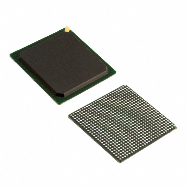
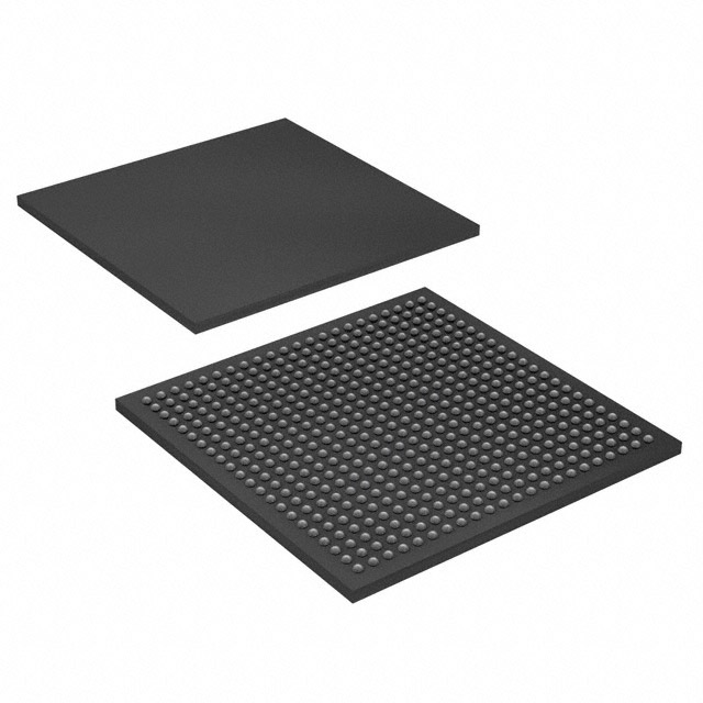
XC4000 Field Programmable Gate Array (FPGA) IC 61 3200 238 84-LCC (J-Lead) |
|---|---|
| Quantity | 320 Available (as of October 7, 2026) |

| Product Category | Field Programmable Gate Array (FPGA) |
|---|---|
| Manufacturer | AMD |
| Manufacturing Status | Obsolete |
| Manufacturer Standard Lead Time | Contact Us |
| Datasheet |
Specifications & Environmental
| Device Package | 84-PLCC (29.31x29.31) | Grade | Commercial | Operating Temperature | 0°C – 85°C | ||
|---|---|---|---|---|---|---|---|
| Package / Case | 84-LCC (J-Lead) | Number of I/O | 61 | Voltage | 4.75 V - 5.25 V | ||
| Mounting Method | Surface Mount | RoHS Compliance | RoHS non-compliant | REACH Compliance | REACH Unaffected | ||
| Moisture Sensitivity Level | 3 (168 Hours) | Number of LABs/CLBs | 100 | Number of Logic Elements/Cells | 238 | ||
| Number of Gates | 3000 | ECCN | EAR99 | HTS Code | 8542.39.0001 | ||
| Qualification | N/A | Total RAM Bits | 3200 |
Overview of XC4003-6PC84C – XC4000 Field Programmable Gate Array, 84-LCC (J-Lead)
The XC4003-6PC84C is a commercial-grade Field Programmable Gate Array (FPGA) from the XC4000 family, delivered in an 84‑lead LCC (J‑Lead) surface-mount package. It combines a regular CLB-based programmable architecture with on-chip RAM and a perimeter of I/O to support custom digital logic and system integration tasks.
Designed for rapid development and reprogrammability, this device targets prototyping, control and interface logic, and medium-density digital designs where 100 CLBs, approximately 3,200 bits of embedded RAM and 61 I/O pins provide a compact, configurable solution. The device operates from a 4.75 V to 5.25 V supply and across a 0 °C to 85 °C commercial temperature range.
Key Features
- Core architecture — 100 configurable logic blocks (CLBs) and 238 logic-element cells give flexible combinational and sequential logic resources for custom functions.
- Embedded memory — Approximately 3,200 bits of on-chip RAM support small data buffers, FIFOs and lookup tables within the fabric.
- I/O capacity — 61 user I/O pins around the device perimeter enable interfacing to peripherals, buses and control signals.
- Logic density — Approximately 3,000 equivalent gates for medium-density logic implementations.
- Power and supply — Operates from a 4.75 V to 5.25 V supply range, suitable for 5 V systems.
- Package and mounting — 84‑lead LCC (J‑Lead) surface-mount package; supplier device package listed as 84‑PLCC (29.31 × 29.31 mm).
- System-level features (family) — XC4000 family capabilities include on-chip ultra-fast RAM, dedicated high-speed carry-propagation circuitry, wide edge decoders and an internal low-skew global clock/signal distribution network, supporting complex logic and timing-sensitive functions.
- Configurability — Family-level support for unlimited reprogrammability and multiple programming modes enables iterative development and field updates.
- Environmental — RoHS compliant; commercial operating temperature range 0 °C to 85 °C.
Typical Applications
- Prototyping and development — Unlimited reprogrammability and the XC4000 family architecture accelerate iterative design and functional verification.
- Custom control and glue logic — 61 I/O lines and 100 CLBs enable implementation of control state machines, bus adapters and interface bridging.
- Embedded data buffering — Approximately 3,200 bits of embedded RAM support small FIFOs, LUT-based storage and temporary data buffers.
- Medium-density digital functions — With ~3,000 gates and dedicated arithmetic carry paths, the device handles arithmetic logic, counters and timing logic in compact systems.
Unique Advantages
- Reprogrammable hardware: Unlimited reprogramming capability from the XC4000 family lets designers iterate quickly without changing PCB hardware.
- Balanced resource mix: The combination of 100 CLBs, 238 logic-element cells and ~3,200 bits of RAM supports a wide range of medium-density designs while keeping board area compact.
- Robust I/O: Sixty-one user I/Os provide straightforward connectivity for peripherals, sensors and external logic without external glue chips.
- Straightforward integration: Surface-mount 84‑lead LCC (J‑Lead) package and standard 5 V supply simplify mechanical and power design for commercial applications.
- Regulatory and assembly friendliness: RoHS compliance aids in meeting environmental requirements for commercial products.
Why Choose XC4003-6PC84C?
The XC4003-6PC84C positions itself as a practical, reprogrammable FPGA for commercial applications that require medium-density logic, embedded RAM and a substantial I/O count in a compact surface-mount package. Its family-level architectural features—including carry-propagation support and a global clock distribution network—help implement timing-sensitive and arithmetic functions while the on-chip RAM and CLBs reduce external component count.
This part is well suited to design teams and procurement looking for a configurable solution that accelerates development cycles, supports iterative firmware/hardware updates, and provides a clear upgrade path within the XC4000 family for scaling functionality.
Request a quote or submit an inquiry to receive pricing and availability information for XC4003-6PC84C and to begin evaluation or procurement.























Date Founded: 1969
Headquarters: Santa Clara, California, USA
Employees: 25,000+
Revenue: $22.68 Billion
Certifications and Memberships: ISO9001:2015, RoHS, REACH











